How to Optimize PCB Design for SMT Assembly Process Flow
Key Takeaways
-
Learn the basics of SMT assembly process flow.
-
Find out why optimizing for SMT assembly is important.
-
Explore ways to optimize PCBs for SMT assembly.
SMT assembly includes a series process to populate and solder components on a PCB
Even in my late 30s, I’m still a huge fan of the Transformers franchise. I’ll clear my schedule just to be the first to catch Optimus Prime and co. on the big screen. Obviously, I’m on the side of the Autobots, and the sight of them assembling in the desert scene of the 2014 classic, Age Of Extinction, is a sight to behold.
However, assembling hundreds of surface mount technology (SMT) components on a PCB offers a different kind of excitement compared to seeing towering robots on screen. Besides marveling at the technologies that handle such tiny parts, there’s also the diligently carried out optimization to ensure the process goes smoothly.
Understanding the SMT Assembly Process Flow
It’s rare for a PCB designer to step into a PCB assembly facility and try to handle the process themselves. Still, it helps to understand what happens behind the scenes where reels of components are transferred onto bare PCBs and carefully soldered.
The SMT assembly process starts with the supplier getting ahold of the Gerber file, or other placement data, from the designer along with the PCBs and components. Gerber files are used to configure the various machines used in the assembly process, such as placement and optical inspection. Suppliers also use the Gerber data to create stencils that are used to apply solder paste on the PCB. The stencil is held tightly onto the PCB and solder paste is injected onto the pads through an applicator machine.
The next process involves picking and placing the components on their designated footprints. A placement machine picks up the component from a reel or tray using a vacuum nozzle. The components are then accurately placed onto the PCB with the guidance of high-accuracy optical technology.
As all the components are transferred onto the PCB, they are inspected optically with a machine to ensure there are no mistakes prior to reflow soldering. Once that’s done, the PCBs are moved to a reflow machine where they are heated up to melt the solder on the paste. The process connects the pads and pins of the components.
Before the PCBs are delivered for testing, they are inspected with machines with optical, and in some cases, X-ray technologies. The inspection is an important step to detect bad solder joints or short circuits that can occur during the reflow process.
Why Do You Need to Optimize PCB Design for the SMT Assembly Process?
Optimization prevents issues affecting SMT assembly
It may seem that SMT assembly has very little to do with PCB design. In reality, decisions made during design can influence the assembly process. From your choice of components to their arrangement on the PCB, SMT assembly can be a smooth process or quite the opposite.
For example, omitting fiducial marks will lead to difficulty in accurately placing QFP or BGA type components on the PCB. Fiducial marks, which are located at the corners of a PCB or component, are used by the optical system to pinpoint the coordinates of a given component with a high degree accuracy.
You can also run into trouble if you’re oblivious to the fact that placement machines will need to have a firm grip on the PCB. If you’ve populated components on the edge of the PCB, there aren’t any areas left for the machines to grip, which may affect the SMT assembly process.
How to Optimize Your Design for SMT Assembly Process Flow
Fiducial marks ensure accuracy in the pick and place process.
Obviously, you’ll need to add in the fiducial marks if you haven’t already done so. While some modern machines may be able to work without any, you can’t assume that is going to be the case for your supplier. At the very least, place fiducial markers at the corners of the PCB.
Tooling strips are equally important, especially if you’re tight on space on the PCB. Create tooling strips of 6 mm minimum to allow the machines ample grip during assembly. Adding V-score on the strips makes it easy for the parts to be broken off later.
Another fundamental practice is to have the SMT components aligned in a single direction. This is important, especially for components with pin 1 designation. Doing so prevents mistakes and allows component placement to be done in a single run.
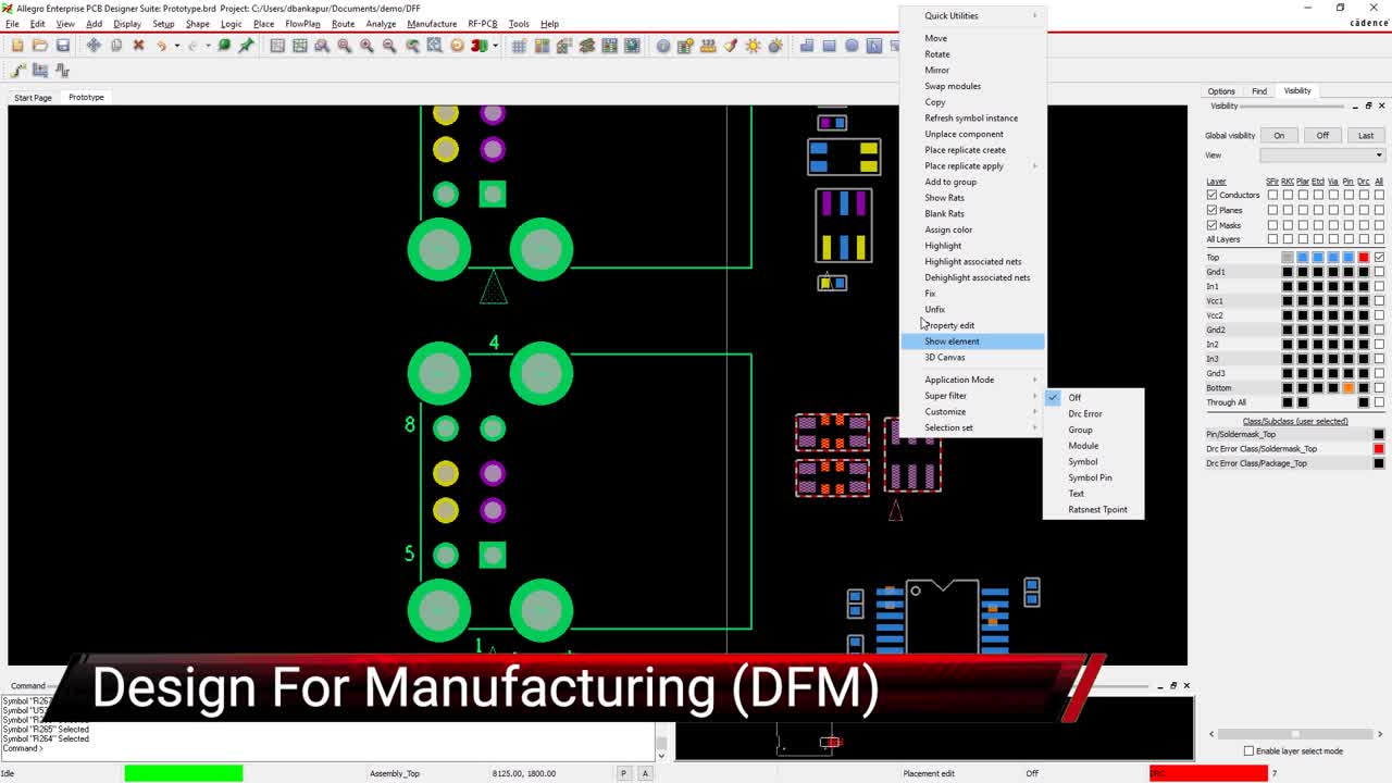
These optimizations aren’t difficult if you’re using the right PCB design and analysis software. Cadence Allegro, which allows you to set assembly rules, prevents missing out on essential SMT assembly optimizations.
If you’re looking to learn more about how Cadence has the solution for you, talk to us and our team of experts.