Comparing SGMII vs. SerDes Trace Routing for Communications PCBs
Key Takeaways
-
What are communications boards?
-
What are SGMII and SerDes?
-
Trace routing for PCB layouts with SGMII vs. SerDes interface connectivity.
Proper communication is important.
When I was a teenager, we had a cat and a dog, both of which we got when they were very young. I guess you could say they grew up together as sisters. Naturally, they had their disagreements, with Friskie (a domestic longhair) perched on a dresser or table periodically meowing, and Lady (a german shepherd) below on her hind legs barking. These encounters were intriguing because it was obvious they had no real intent to do any harm. Instead, they seemed to be trying to make their case with each not understanding the other’s language.
Unlike most animals, people have mostly solved their language barriers through translation. However, lack of communication can still exist when transmitting and receiving data between electronic networks. Since its public introduction, Ethernet, invented by Bob Metcalfe in 1973, has grown to be the standard for wired network connectivity, enabling various electronic systems, devices, and boards to communicate.
Many advances have been made to Ethernet over the years to increase the data rate or throughput between networking boards and to improve connectivity with on-board components and modules. Two of these advancements are serial gigabit media-independent interface (SGMII) and serializer deserializer (SerDes), both of which are used for high-speed board communications that require special trace routing considerations. First, let’s see why communications PCBAs are special, then compare the routing considerations of SGMII vs. SerDes, and, lastly, see how to best design your PCB layout for boards that utilize SGMII and SerDes for network connectivity.
Why Are Communications PCBAs Special?
Throughout your career as a circuit board designer, you will likely be called upon to create PCB layouts for many different types of boards. To excel at this necessitates not only an understanding of the board’s intended functionality but also how to design, incorporating aspects to improve design manufacturability that may vary among board types. Communications boards are one of the types where special consideration is warranted, as illustrated below.
The list above is not exhaustive, as trace routing is also a special consideration for communications boards. Depending upon the type of components and the signals routed to and from them, trace length, copper weight, and spacing must all be chosen to maximize signal integrity. Routing between connectors on a board and between boards is critical for the successful operation of the PCBA and networking with other electronic boards and systems, as demonstrated by the utilization of SGMII and SerDes, discussed below.
What Is SGMII and SerDes Connectivity?
Media independent interconnect (MII) is an Ethernet standard, defined in IEEE 802.3, for connecting a media access control block (MAC) to the physical layer (PHY) of the seven-layer OSI network interface controller (NIC) for networking. SGMII performs the same task, extended to include gigabit Ethernet, although it can be used for 10/100 Mbit/s TX/RX as well. SerDes technology, which is often used with SGMII, provides LVDS (low-voltage differential signaling) for converting between serial and parallel signal routing, as shown in the figure below.
SGMII vs. SerDes example implementations.
As shown in the figure above, SGMII may be used for component interconnectivity on the PCBA or between multiple boards. SerDes is used similarly on PCBAs where there is limited pin availability for I/O; however, for cabling or multi-board connection, TX/RX is typically serial. Now that we know how these connectivity technologies are used for communications boards, let’s see how best to lay out the boards.
PCB Layout Routing for SGMII vs. SerDes
Depending upon the type of data being processed, communications boards may be populated by various types of processors, which typically are high-pin count and high-heat-generating devices. This means that optimizing space is a priority, as is thermal distribution and dissipation. For boards that implement HDI, spacing and temperature concerns are exasperated.
Another major concern for many communications boards is impedance mismatches, which can result in signal degradation and dropped or lost data. Impedance matching between copper traces is critical for differential routing and between the board materials for high-speed (frequency) signal transmission. Due to these and other concerns, the following guidelines should be followed when laying out out your PCBA with SGMII and SerDes connectivity.
SGMII vs. SerDes PCB Layout Guidelines:
☐ Make sure that traces are equally spaced from each other.
☐ Make sure that copper weights are the same for all traces.
☐ Make sure that trace lengths are the same. Use meandering if necessary.
☐ Avoid impedance mismatches.
☐ Choose materials with matching dielectric constants.
☐ Minimize the length of parallel traces to maximize the use of space.
☐ Follow your contract manufacturer’s (CM’s) design for manufacturing (DFM) for clearances to minimize EMI.
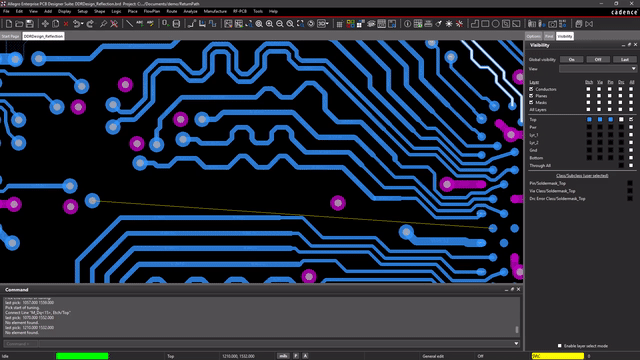
Following these guidelines will help optimize the performance and manufacturability of your PCBAs when using SGMII and SerDes. To create the best design, you need to be able to thoroughly review and evaluate your layout, preferably in 3D, as shown below.
3D PCB layout routing and inspection with Allegro Designer.
Additionally, thermal analysis and simulation should be performed to ensure that your board’s heat profile is not a concern for board assembly or it will be subject to premature failure once in the field.
Cadence’s PCB Design and Analysis package, including Allegro PCB Designer, is the most comprehensive design tool in the industry. It enables 3D analysis and review throughout design, allowing you to send your design off with the confidence that it meets its design intent and your CM’s specifications.
If you’re looking to learn more about how Cadence has the solution for you, talk to us and our team of experts.