Signal Integrity Basics and Fundamentals in PCB Layout
Key Takeaways
-
Exploring the basic principles of signal integrity
-
Fundamental PCB layout techniques for maintaining signal integrity
-
Essential tools and features to improve signal integrity in designs
Understanding signal integrity basics is important for anyone involved in PCB design. Signal integrity refers to the quality of an electrical signal as it travels through a circuit, impacting whether it reaches its destination without degradation. For those new to the concept, signal integrity issues can lead to various operational problems, from minor disruptions to complete device failure. This guide will review the fundamentals, highlighting key principles and practical steps for achieving optimal signal quality. This involves every aspect of PCB design, including the parts used, the fabrication of the raw circuit board, and how the parts are arranged and connected.
Signal Integrity Basics: Avoiding Potential Problems
There may be occasional glitches in performance, a piece of data may be dropped, or the device may even fail to operate in extreme cases. All of these issues can often be traced back to signal integrity problems.
As signal speeds increase in our electronics, they are more susceptible to various aggressive interferences. These can include signal reflections due to the following:
-
ground bounce,
-
and crosstalk.
If the circuit board is not specifically laid out to counter these problems, signal degradation may continue until it no longer works as designed. Additionally, the circuit board must be designed to not create signal integrity problems for its own circuitry or nearby electronics. Before we look at how to design for these problems, let's first examine some critical signal integrity fundamentals.
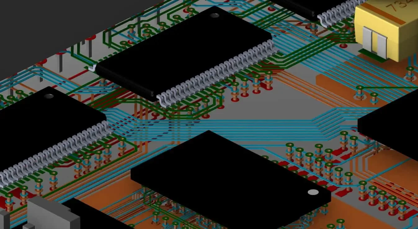
Signal integrity fundamentals are critical to the success of circuit boards like this.
Understanding The Basics of Signal Integrity Fundamentals
A signal on a circuit board can have its quality degraded due to several effects, which can be categorized into different groups. Here are four main areas of poor signal integrity that you should be aware of.
Electromagnetic Interference (EMI)
In the context of PCB design basics, EMI is a form of interference caused by unwanted electrical signals that can disrupt the performance of nearby electronics. High-speed signals often produce EMI if not properly managed, leading to noise in the circuit or even signal loss.
-
Not only can the length and configuration of the traces be a problem, but trace and via stubs can also act as an antenna.
-
Another source of EMI is the signal return path, which should optimally be on an adjacent reference plane. If the return path is blocked, the signal will radiate even more noise as it seeks a path back to its source.
Unintentional Electromagnetic Coupling (Crosstalk)
Crosstalk happens when signals on closely routed traces unintentionally interact, potentially causing one signal to interfere with another. Imagine two conversations happening side-by-side. If the speakers are too close, they might overhear each other and get distracted. Similarly, when traces on a circuit board are too close, one signal might unintentionally “hear” another, causing interference.
-
For PCB design beginners, routing traces at an adequate distance apart is a foundational technique for mitigating crosstalk, especially on high-speed designs.
-
This problem occurs with side-by-side traces and traces routed in parallel on adjacent board layers. This type of crosstalk is known as broadside coupling, which is why most circuit board designs alternate horizontal and vertical routing directions on adjacent layers.
Simultaneous Switching Noise (Ground Bounce)
With many components switching between high and low states on a circuit board, the voltage level may not return to the ground potential as it should when it switches low. If the voltage level of the low state bounces too high, the low state of the signal may be falsely interpreted as a high state. When a lot of this happens simultaneously, it may result in false or double switching and disrupt the operation of the circuit.
-
To manage this, designers ensure proper spacing of components and avoid blocking return paths.
Impedance Mismatch
In signal integrity basics, an impedance mismatch occurs when the electrical resistance (impedance) along a trace varies. This is primarily relevant in high-speed signals that input/output into an IC. This difference causes signal reflections, leading to signal distortion. Think of trace impedance as a road for signals. If a road suddenly narrows, it causes traffic to slow down or back up—similar to how mismatched impedance causes signal reflections:
-
Designers can manage this by configuring the trace width and adjacent layers for consistent impedance. Learning these basics helps prevent signal integrity issues and ensures clean signal transmission.
-
Properly routing impedance-controlled sensitive traces requires a specific layer configuration, trace width, and clearance.
With the major problems in signal integrity defined, let’s now look at some PCB design techniques that will offset some of these issues.
PCB Layer Configurations and Component Placement
For beginners, basic component placement is essential for signal paths and reducing EMI. Place components logically from source to destination, aligning with the schematic to simplify routing.
Signal integrity problems in printed circuit boards are often due to improper signal return paths. Not only does the return path need to be free of obstructions, but it also needs to be on an adjacent reference plane layer for the best signal integrity. This configuration requires arranging the board layer stackup with dedicated layers for sensitive high-speed routing and adjacent reference planes in a microstrip or stripline configuration. A basic microstrip setup involves routing surface traces with an adjacent plane, while stripline configurations sandwich traces between two planes to reduce interference further.
Microstrip and stripline layer configurations factor into signal integrity
While all signals will benefit from having an adjacent reference plane for a clear return path, it becomes even more important for sensitive signals routed with controlled impedance. Calculating the dielectric constant, width, and trace thickness will determine the trace width for controlled impedance routing. Since changing the board layer stackup or the materials used for PCB fabrication will alter these calculations, designers must determine the board layout configuration before the layout begins. These calculations will also vary depending on whether or not the impedance-controlled traces are routed using one of several microstrip or stripline configurations, as shown above.
With the board layer stackup configuration determined, the next step is to place the components on the board. Many high-speed circuits consist of multiple nets, which start at the source or driver pin on one component, continue through other parts, and terminate at the final component's load pin. These circuits are referred to as signal paths. To maintain their signal integrity, they must have their parts placed in sequence, as detailed in the schematic, to allow for the shortest point-to-point connection between pins. Other components, such as processors and memory chips, need to be spaced far enough apart to allow all their routing topologies yet close enough for short connections. Here are some other key points of component placement to remember:
- Follow the logic flow of the schematic when placing high-speed circuitry.
- Place bypass capacitors close to each power pin of processor and memory devices.
- Allow room for escape routing and bus routing.
- Adhere to your assembler’s design for manufacturability (DFM) rules.
- Ensure that the heat of hot-running components is dissipated.
With the parts on the board, the next step is routing.
Circuit Board Trace Routing and Reference Planes
Differential pair routing on a circuit board
At this point, you will be ready to start trace routing but remember that trace routing is closely tied to how the components are positioned for good signal integrity. Escape routing, for instance, has to be carefully designed to ensure that all the signals are connected and that associated components, like bypass caps, are as close to their pins as possible. Many designs rely on via-in-pad for large pin-count BGAs to keep connections short and open up more room for routing.
|
Section |
Guidelines |
|
Trace Routing Readiness |
|
|
Routing High-Speed Circuits |
|
|
Differential Pairs |
|
|
Length-Matched Nets |
|
|
Avoid Noisy Areas |
|
|
Room for Routing Topologies |
|
|
Minimize Via Usage |
|
In addition to the routing, you will also need to design the board’s power delivery network (PDN). At its core, a stable PDN is critical for signal integrity. For beginners, this means creating straightforward pathways for power with minimal noise, preventing any signal distortions.
It is also critical that you do not route high-speed transmission lines through areas of blockage on the reference plane. This can increase the amount of EMI the board generates as the signals wander around, trying to find a clear return path to their source. Blockages can include split planes, board cutouts, or dense areas of vias, as shown in the picture below.
Dense areas of vias can create a blockage for signal return paths on a reference plane
Designing a circuit board that maintains good signal integrity is a lot of work. Fortunately, your CAD tools have some excellent features that can help.
Layout Tools That Can Help Designers Maintain Signal Integrity
OrCAD X has features that ensure signal integrity is maintained in designs. OrCAD X provides advanced routing options, constraint management, and 3D design visualization tools that support optimal signal routing and adherence to signal integrity principles. OrCAD X Workflow Manager for Signal Integrity allows designers to set up and analyze impedance workflows, aiding in configuring net-based and directed group analyses to maintain consistent impedance and minimize signal loss. For more information on high-speed design and signal integrity fundamentals, look at this E-book.
|
Capability |
Description |
Signal Integrity Aid |
|
Impedance Workflow Manager |
Provides tools to set up impedance workflows, allowing net-based or directed group impedance analyses. |
|
|
Constraint Management |
Offers control over trace widths, spacing, and via use, with specific settings for high-speed signals. |
|
|
3D Visualization |
Allows real-time 3D design views, verifying component placement and layer stackup integrity. |
|
For designers aiming to follow signal integrity basics for PCB layouts, Cadence tools, specifically OrCAD, offer comprehensive solutions to tackle complex signal challenges. To learn more about Cadence’s full suite of tools for PCB design and signal analysis, explore the PCB Design and Analysis Software page or dive into the details of OrCAD X.