Best Practices for Capturing Circuit Board Schematics
Key Takeaways
-
Schematic database and library preparations
-
Schematic capture best practices and recommendations
-
Finalizing the schematic in preparation for PCB layout
A printed circuit board sitting on its schematic
Everyone knows that the most productive way to shop for groceries is to prepare a shopping list before you go. Not only will you save money and move faster, but it can help you to say “no” to tempting items that may not be a part of your diet. Preparing a written plan like this can help any project that we’re involved with, and, in electronics, these plans are known as schematics.
Schematics detail the circuitry that is built into and installed on a printed circuit board. Originally hand-drawn on a drafting table, schematics are now created using computer-aided design tools. These CAD systems are also tied together with PCB layout tools, circuit simulators, and parts procurement systems for the overall design of the entire circuit board. No matter how much automation is involved, it is still incumbent on electronics designers to carefully produce a clean and readable schematic. To that end, here are some best practices that can help when capturing circuit board schematics.
Preparations for Capturing Circuit Board Schematics
The first step in creating an organized schematic is to be familiar with your CAD tools and comfortable using them. Spending hours trying to execute simple commands is a recipe for frustration that can negatively impact your work. Fortunately, there are many ways to resolve this problem, from online training courses by the vendor, user groups, white papers, and instructional videos. In addition, taking the time to learn your tools will pay huge dividends in productivity.
Your CAD tools will also need to be prepared for the work that you will be doing. Although they will operate straight out of the box, most people customize their tools for both ease of use and to maximize their productivity. Here are some of the CAD system customizations that you should consider:
- Parameters: These can be adjusted to change colors, grids, and a host of other settings. An example of some parameter settings can be seen in the picture below. These settings can usually be saved or read in automatically by the tools as startup files.
- Templates: Most companies will want their contact and legal information included on the schematic sheets. These can often be generated by the CAD system or by reading in a sheet template with the information already in place.
- Design rules: Most companies will work from an established set of design rules that can be altered for each design. As with the other setups, design rules and constraints are usually read in automatically upon startup or available through a readme file.
- Library links: These links are normally read in automatically, although designers will often attach manually to new library links as required for a unique part.
In addition to preparing the CAD tools for schematic capture, there are also other steps that a designer needs to take before getting started. These include working together with the other design team members to coordinate between the software and mechanical portions of the design. The designer should also have the physical parameters of the PCB decided on before starting, as these will impact the circuitry being designed. Although these parameters often change during design, it is still a good practice to start with the size, shape, and layer stackup of the board as close as possible to the final product. It is also beneficial to involve the circuit board manufacturer at this point to ensure that the board can be built as designed.
With the parameters set, the next step is to prepare the library parts that will be used in the schematic.
Some of the schematic parameters that can be set up in a CAD system
A Well-Developed Library of Schematic Symbols and Parts Is Essential
Creating your schematic requires that you have all of the symbols you need available for you to work with. These symbols can either be imported or built within the CAD system using the built-in drafting capabilities for drawing lines, circles, and polygons. Symbol-building tools will also allow you to create text and assign electrical properties. The key to building a correct symbol is to work from the most current part information available, which will require a little research. Another option is to use the automated tools within the CAD system to generate the symbols. These symbol creation wizards use industry standards to create the proper sizes and shapes.
In addition to the symbol, there are other portions of the part that go into making a complete component. This includes the physical footprint for PCB layout, the electrical parameters that connect the schematic symbol to the PCB footprint, and simulation and 3D models. All of this information should be saved into a library that the designer can access, and many companies use a combination of both project and corporate libraries for more efficient library organization.
There is also another method of gathering all of the library data you need, and that is to use a third-party library service. These providers offer online catalogs that list thousands of parts they have available, allowing the designer to select and download the symbols, footprints, and 3D models of the desired part. These library providers are also often available from within your schematic capture tools, as shown in the picture below. Here you can see that an EEPROM has been selected, allowing the designer to open its datasheet and image files and view the part information, symbol, and footprint as well. This part can then be pulled into the schematic and all of the required data files will be automatically saved within the session.
Once you have gathered your library parts, it’s time to start capturing the schematic.
The Unified Part Search tools in Cadence Allegro
Circuit Board Schematic Capture
Schematic capture not only serves as a foundation for the electrical connectivity of circuit board design, but it is also a legal document. Therefore, the schematic must be correct electrically, and it also has to be readable and usable for other design team members, manufactures, technicians, and end-users. To accomplish all of this, here are the main steps that you need to focus on as you capture the circuit board schematic.
Logic Flow
The logic flow and connectivity must be consistent and easily understood as you lay out the symbols and their connected nets. This is very important for high-speed circuitry, where the PCB layout team will need to design signal paths based on the logic flow of your schematic.
Give Yourself Room
Make sure to leave yourself plenty of room when you place symbols on the schematic sheet. Not only will you have a lot of nets that need to be drawn from pin to pin, but those nets will also have names and pin numbers that need to be legible.
Editing
Don’t be afraid to move your symbols and nets around on the schematic sheets to create room. Your schematic capture system will have powerful features available for maneuvering symbols and nets as well as cutting and pasting areas of circuitry. Make sure that all of your reference designators, part numbers, values, and additional text are not covered up by other schematic objects. Remember that the objective is to make a readable and usable schematic and not to save paper.
Design Rules and Constraints
Although most design rules won’t come into play until the design is ready for PCB layout, it is a good idea to create different net and component classes now. This will allow you to assign specific design constraints to these classes that you want the layout team to know about and follow.
Properties
There may be properties that have to be adjusted in the schematic as you are working. Make sure that you use the property editor to do this, as demonstrated in the picture below. Here the property editor in Cadence’s Allegro Design Entry CIS tools is being used to adjust the values of a selected part.
Text Information
In addition to the circuitry, a schematic should also contain essential information for the company and the circuit board. This data will include part numbers, product information, revision numbers, and company contact and copyright information.
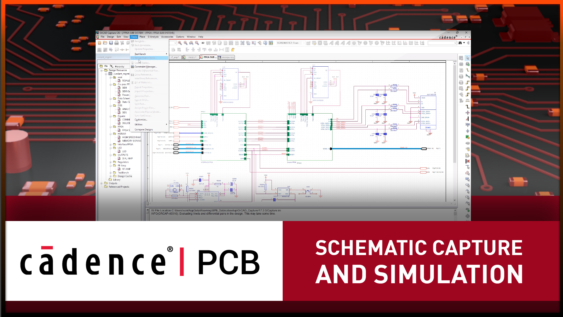
DRCs
It is imperative to run the design rule checks in a schematic while designing it and then again before sending it to PCB layout. This will prevent obvious errors, such as missing pin connections, from getting all the way to manufacturing.
Not only does the schematic have to be readable, but it has to be usable from a CAD tool perspective as well. Creating a clean and organized schematic will help with that, as will running the design rule checks to ensure that the schematic database does not carry any errors into layout. At this point, the schematic is almost ready for layout, but there are still a couple of things to do first.
The property editor opened on a selected component
Simulation and PCB Layout
Up to this point, the schematic capture process has been focused on producing a clean circuit board schematic without any connectivity errors. However, there is still the question of how well these circuits will perform as designed. To find out, it is best to run the schematic through circuit simulation using your CAD system’s SPICE tools. This will tell you whether or not your circuits will work as they are designed, predict their behavior while the board is operating, and expose unexpected behaviors in the circuits. SPICE tools also allow you to investigate different circuit design options without investing time and money in physical parts and labor to build breadboards or prototypes.
Now you are ready to transition the schematic to layout and to do that, you need to prepare your design for this last step. This includes running final design rule checks and ensuring that all the required properties, text, and circuit connectivity have been captured correctly. With those preparations complete, you can create all of the data files needed to transfer the circuit board schematic into the layout and begin that stage of the PCB design.
For more information on schematic capture, please check out this E-book.
If you’re looking to learn more about how Cadence has the solution for you, talk to us and our team of experts.