PCB Component Placement Defect Detection for Layouts
Key Takeaways
-
Common component placement errors that create problems during PCB assembly
-
Different PCB component placement defect detection methods you can use
-
Getting the most out of your PCB design tools to detect placement errors
Wouldn’t it be nice if every printed circuit board we laid out had lots of space where we could spread the components out with plenty of room for routing, vias, and text? Dare to dream, I’m afraid. The truth is that the majority of the circuit boards we design will try to include as much circuitry and functionality as possible. Our job is to find a way to make it all fit on the board while obeying all of the applicable rules and constraints for the design.
With PCB space at a premium, it’s not unheard of to miss some minute details during component placement that could lead to problems during manufacturing. Sometimes, these difficulties will originate with the component footprints that we are using before component placement even begins. Let’s take a closer look at all of this, starting with some of the more common problems resulting from bad footprint data or incorrectly placed components on the board. Then, we’ll examine some ways that can help enhance PCB component placement defect detection during circuit board layout.
PCB Component Footprints: More Than Just a CAD Representation
Component defect detection begins with using the correct CAD footprint models
Many of the problems that slow or even stop circuit board manufacturing are due to incorrectly designed component footprint models in the PCB design CAD system. Many years ago, designers could get away with a lot of slop in their footprint patterns due to the larger sizes of the parts and less stringent design rules. However, today, that same lack of attention to detail can end up causing a lot of problems. Here are some of the issues that can arise when component footprints are not built correctly:
-
Inadequate clearances: Component outlines and pad patterns can inadvertently cause clearance problems to neighboring components on the board if they are created incorrectly. An outline that is too small could result in insufficient room for the parts to be placed next to each other.
-
Poor solder joints: Surface mount pads that are incorrectly located and sized in the footprint can lead to soldering problems. Solder fillets may not correctly form if there isn’t enough room on the pads for the leads to sit on, or the part may “float” off the pads if there is too much room. Thru-hole pins may have difficulty being inserted into drill holes that are too small or holding onto a solder joint if the hole is too large.
-
Functional problems: The components assembled to the board will not work if the pad patterns they are soldered to are not numbered correctly. In some cases, this could even result in a catastrophic failure such as a fire.
-
Test, debug, and re-work issues: Without enough space between components or pad patterns, the technicians testing and re-working the board will not have enough room to do their job.
It is imperative to correctly build these footprint models in the CAD system before layout starts. Many PCB design CAD tools have automated tools built into them to help with footprint creation, and designers should use these as much as possible.
Once the component footprints have been verified as correct, it is time to start placing parts on the board. Once again though, the potential for creating manufacturing problems exists if the components are not placed correctly.
The Problems Resulting From Incorrect Component Placement
While there are still some designs where you can spread out the components during placement, most of the time you will be trying to find enough room to get all the parts on the board. At the same time, you will also have to obey circuitry constraints for electrical performance and DFM rules to ensure the board’s manufacturability. If these rules are not followed, your manufacturer may run into the following problems during PCB assembly:
-
Clearance violations: Placing parts too close to each other may cause difficulty for the automated pick and place machines when installing components on the board. Inadequate clearances can also hurt the board’s ability to go through automated testing, and it can create problems for the technicians that have to debug and re-work the board.
-
Location errors: Placing components in the incorrect position and rotation can create wave soldering equipment problems. Taller components that proceed shorter ones into the wave may shadow the smaller parts and prevent them from being completely soldered. Components must also be aligned correctly for their land patterns to get evenly soldered. Taller parts on the bottom of the board may also have difficulty going through the wave and require special fixtures or manual assembly later on.
-
Configuration problems: Smaller two-pin components going through the solder reflow oven can be susceptible to an effect known as “tombstoning” if the metal connecting the two pads is not balanced. The pad with a greater amount of metal will draw the heat out, causing the solder on the other pad to melt faster. This unbalanced melting can sometimes pull the part off the unmelted pad and stand it up like a tombstone.
Many other problems can arise from incorrectly placed components. These range from human inaccessibility to conflicts with other system objects such as brackets and system enclosures. You can use some tools to help you detect these problems while the board is still in layout, and we will examine those next.
Careful placement of parts like these are important for making the design manufacturable
PCB Component Placement Defect Detection Methods
To avoid problems with components that violate DFM rules, designers need to detect these problems in layout before the board is manufactured. The first line of defense against these errors is to use the design rule checking system built into your PCB design CAD tools. These checks use the design rules and constraints you can set up within the tools, and you can help yourself by setting up as many of these as possible.
In modern PCB design CAD tools, you will have the ability to set up rules and constraints for the following conditions:
-
Component to component spacing
-
Component class to class spacing
-
Rules for specific areas
-
Silkscreen, solder mask, and solder paste constraints
With these rules and constraints, you will be able to place your component footprints on the board with the minimum spacing requirements for manufacturability being automatically managed. Additionally, most tools now have the ability to view and check the design in 3D. By importing the board’s mechanical features along with other system boards and enclosures, you can thoroughly check the design for errors. This includes checking for parts that are too close to other system features such as switches or connectors or verifying that none of your taller electrolytic capacitors are inadvertently poking up through the system enclosure.
The key to success with these PCB component placement defect detection methods is making sure that they are used to their fullest capacity. Let’s take a look at how to do this using Cadence’s Allegro PCB Editor.
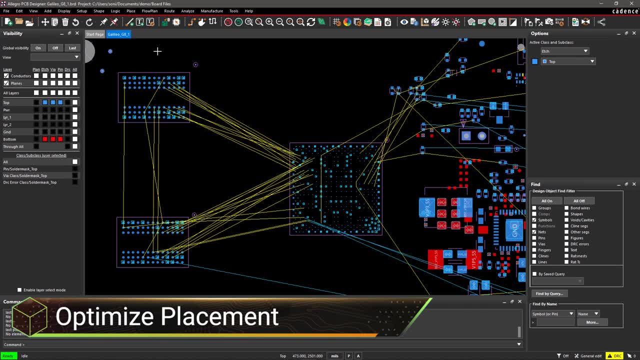
Getting the Most Out of Your PCB Design Tools
The Unified Parts Search menu in Cadence’s Allegro PCB Editor
The first half of PCB component placement defect detection is to ensure that the footprints you are using in your design are built correctly. This starts with ensuring that you are working with current, up-to-date information and diligently building the part according to its specifications. Another good tool to use is the package symbol wizard within Allegro, which will create the component footprint for you from the padstacks, dimensions, and other information that you enter. However, the best tool to use is Allegro’s Unified Parts Search menu, which you can see in the picture above. This tool will find the parts you need online and download the manufacturers’ recommended footprints, symbols, images, and other part-specific information.
The next step in guarding your component placement against defects is to set up the design rules and constraints with all the information needed for accurate placement DRCs.
Using your PCB design CAD tool’s rules and constraints can help to avoid component placement problems
In the picture above, you can see Allegro’s Constraint Manager configured with component spacing values. These can be set up for individual parts or classes of parts to manage the placement clearances that your design needs for manufacturing, helping you with PCB component placement defect detection. These values can be entered manually or imported from a saved set of rules and constraints. Allegro also gives you the ability to import this data from a PCB manufacturer, which will ensure its accuracy and save you time in database setups.
You can find additional information on how best to lay out your printed circuit board according to DFM rules and constraints by reading this E-book.
If you’re looking to learn more about how Cadence has the solution for you, talk to us and our team of experts.