Shorts and Cuts: Post-fabrication Logic Changes
Circuits are usually developed with a few unknowns at the start. Future price and availability of key components is a typical day-one risk. The wise designer leaves themselves some room to future-proof their prototype against the supply chain uncertainty. At the printed circuit board level, risk management generally entails creating separate paths on the P0 (non-form-factor) engineering builds. One path will assess a particular approach and another will facilitate a different answer to the same signal(s).
Zero Ohm Jumpers
A zero ohm resistor is used where the path diverges. While there would only be one resistor, it would have two possible placement options across three pins. In this case, the signal is driven from U11 pin two out to a junction where R2 and R3 overlap. Populating a zero ohm jumper (or a blocking cap) at the R2 location sends the data to C1. Conversely, populating R3 sends the signal to U1. The routing option is then determined by a Bill of Material adjustment. R2 and R3 are mutually exclusive stuffing options.
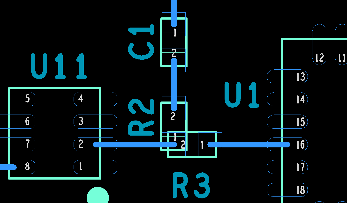
Image credit: Author.
Isolated Ground Return
Ground and Analog Ground are the typical subdivision of the return paths. More complex systems will feature several circuits whose ground pins are tied together then joined to the chassis ground at a single point. Of course, analog to digital converters and their type will have both types of ground on the same device. Different ground domains can exist on the same layer or be paired to separate layers. A ground is a ground except when it isn’t.
Solder Blobs - Sometimes, You Feel Like a Connection; Sometimes, You Don’t.
A normally closed circuit can feature an accessible location for cutting the trace should the need arise. R1 in the image below would be a closed circuit until the trace between the pads is cut. Then a ferrite bead or other component can be placed for effect. A normally open circuit like R4 can have a just-in-case connection that can be made with solder. This is one of many shapes that can be used in this way.
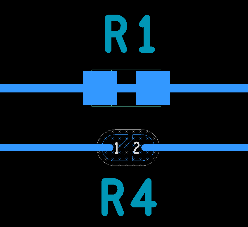
Image credit: Author - A short and an open footprint
Chicken Dots - An Analog Staple
Tuning stubs are another flavor of impedance control. In order to achieve the correct impedance, the RF engineer will resort to a purposeful discontinuity. The requirement for a strong signal at a frequency without too much noise going out as harmonics of that frequency is often a tough problem to solve.
Image credit: Author - note the extra slices of copper just in case.
Giving themselves an out is all part of the job. Copper foil can be added to the seemingly aimless protrusions in order to attenuate the undesirable energy transmissions. Spectral efficiency leads to improvements in power consumption. Likewise, compromised RF design wastes energy by radiating spurious signals. It comes down to win/win or lose/lose.
The live-and-let-live rules from the Federal Communications Commission will prevent you from shipping products that don’t play well with others. One year, we were given T-shirts that compared our amplifiers to black magic. These wireless people are indeed sorcerers in their own way. Little blobs of solder here and there can make or break these things. Of course, the trend is towards more radios to do more cool things. It gets complicated rather quickly.
Oh, the zany stubs we weave wherever analog circuits receive. I’m no Sir Walter Scott but I can say that a lot of RF design involves some deceptive characters. A DC short is also a shunt inductor at 1900 MHz. Let's also break that rule about 90-degree bends and lay down what I named the Picasso for its cubist nature.
Image credit: Author - the “Picasso” shunt inductor
Current Sense and Nonsense
Sometimes, we want to get around a minimum line width for a voltage domain. Enabling a long neck-down as part of the constraint set for a net that carries significant electrical current can and will lead to someone abusing the rule. It could be that infamous auto-router or it could be a future me obeying “the rules”.
A routing challenge will look like this. A voltage net will be constrained to a width considering the current requirement. We would also like a little sample of that power taken right before the Voltage In pin. Run a trace from the load to the “decider” chip. While it can, and should, be a narrow trace, it violates the minimum line width for the net.
Creating an infallible routing solution for routing a narrow trace out of an otherwise wide net can be done by shorting two nets at the desired point. This is often accomplished with a resistor that separates the two nets logically. A via or single-layer pad can be given a property where it can connect two net names at that point even if that point is on an inner layer. Zero ohms costs money.
Net shorts only cost a one-time effort to create them. These tricks are often workarounds if your software tier doesn’t support these wrinkles. Adding a patch layer to the “fool” the artwork or just ignoring the violations can backfire in design reuse. Count on the fact that working designs find new life as a cost-cutting tool.
Fabricators may end up taking shortcuts at times to cut cost, so it’s important to be up front and explicit with your documentation. . Right there on the fab drawing, go ahead and add something like the following.
NOTES: UNLESS OTHERWISE SPECIFIED.
(number). THE FOLLOWING NETS ARE SHORTED TOGETHER. (list of shorts)
Then Do Your Homework
Some hindsight about any of these methods that bend the rules or allow options is that these workarounds should be well-documented somewhere that remains front and center to anyone who comes along to upgrade the design. The silkscreen is a natural vehicle for pointing out the visible functions. An errata sheet that discusses the shenanigans can be placed among the artwork files. Who reads a ReadMe.doc? Almost everyone who has skipped it and then paid the price down the road.
Notes on the schematic regarding splits that occur on inner layers are another method. As a designer, I really appreciate a well-annotated schematic. Let’s say that your EE is sitting down with you to provide some tips on a new layout. Just ask her (or him) if you can open up the schematic and jot some of it down for reference. Maybe even start capturing some constraint sets. They will come to the conclusion that including that data frees them from repeating themselves or losing the intent altogether.
So, be bold. Add that what-if circuit. Make a little opening on the solder mask where you suspect that you might need another shunt capacitor. Wiggle room is an important part of product development. As with any powerful tool, using it comes with responsibility. Take the shortcut but always cover your tracks.