Notes On Schematic Capture
Notes on Schematic Capture
Component libraries are fundamental for designing PCBs. The physical symbol of the footprint for the PCB layout and the electrical symbol for the schematic are married by an attribute that cross-references each respective piece of the puzzle by name. The sacred vows are only complete when all of the pin numbers match. Like the stars in the night sky, the times a net-list has failed to load due to a mismatch between the two items is uncountable.
There once was a time when it was common for the PCB Designer to also capture the schematics. I’m not trying to say that the EE’s came along and broke everything. The simple answer is that once the process involved two or more heads, there are more chances for deviations.
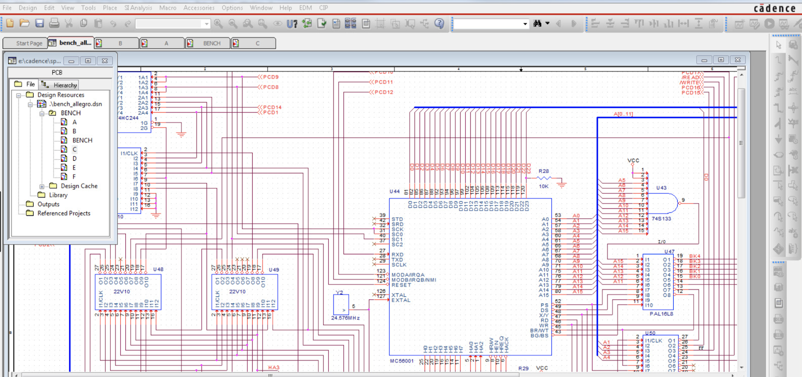
Image Credit: OrCAD
A good hardware team will analyze the schematic, the footprint and perhaps a step-model through the ECAD and MCAD flows to verify a coherent outcome. When you don’t have a team of dedicated librarians, you do it yourself. This article is for you and your small team.
Techs will be pouring over these docs long after our final commit. A radio board layout from the late 1990s is still available online. I’m astonished by the longevity of the “stick” amplifier.
Opening the schematic editor brings up an interface that shares many features of the PCB CAD seat. Likewise, the symbol editor uses similar terminology that is particular to each breed of the tools. Creating a schematic symbol can add a few complications. Unlike creating schematic symbols for resistors and capacitors, there is a level of abstraction necessary to capture components that are housed in Ball Grid Array (BGA) packages.
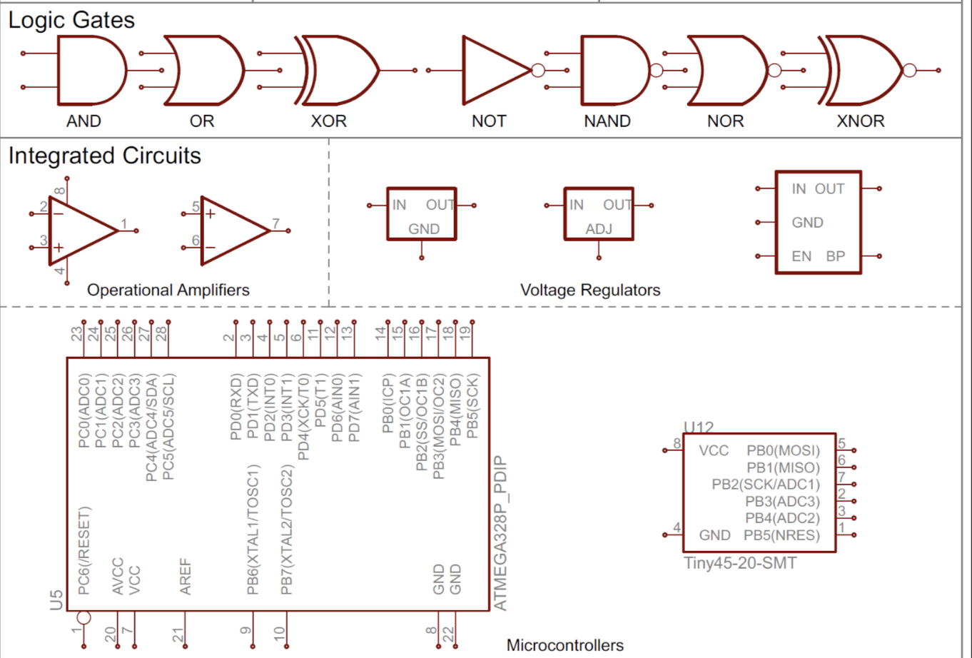
Image credit: Sparkfun
The symbol is defined with one or more rectangles. It is common to try to place the input pins on the left and output pins on the right; with power and ground respectively on the top and bottom. Not all chip technologies behave according to aesthetics so we wind up using some creativity in the actual implementations.
Focus on the pain points
Parts with a high pin-count will occupy a number of boxes that break out as functional blocks. Any bus is likely to be in its own block. When a variety of boxes are used to define one part, the symbol is said to be heterogeneous. Breaking apart into abstract representations is the norm.
Contrast this with the folks of the analog world. When I’m making those symbols, I try to account for the physical layout when that makes more sense. Circulators, couplers, diplexers and the like are simple enough to represent and make debugging easier when the schematic at least vaguely resembles the actual board layout. If you had to look up any of those three RF widgets, good. We have some cool symbols to represent the real world touch points.
Creating all of these pins and making sure they match the ball map in terms of pin numbers is one part. The other is defining the pin type. These attributes do more than decorate an otherwise boring box.
Sorting For Simulation (and face it, YOU WILL BE SIMULATED!)
The pin type comes up in lists when assigning other attributes. That’s when it is handy to know a driver from a receiver. More than that, there are bidirectional pins (think GPIOs) clocks, inverted signals, tri-state outputs and so on.
Spend the time to define and document your process to make life easier down the road. Techs will be pouring over these docs long after your final commit. A radio board layout from the late 1990s is still available online. I’m astonished by the longevity of the “stick” amplifier.
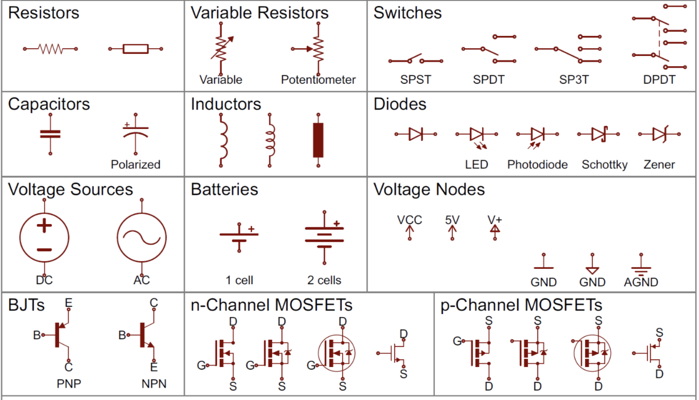
Image credit: Sparkfun
Maybe, you skipped all that and used a CAD library service. There may still be some refinement of the symbols to be usable in your system. The library service will give you a leg up but ultimately, you own the design. That means that the test drive is up to you even if the parts are certified as compliant. The quality of the board depends directly on the quality of the various symbols.
With all or most of the symbols created, it is time to do some schematic capture. Some of the information attached to the schematic symbol is always visible. Those are the reference designators, the part value and optionally, the tolerance and rating of the part. You may have seen schematics with more or fewer visible attributes.
There are usually a few that remain invisible including the footprint itself and the part number. Those two are extracted for the netlist and the bill of materials. No-connect pins are usually included in the symbol but sometimes they are embedded such that they are invisible. Most (sane) people want to see all of the pins represented visually.
Symbol Placement
Placing symbols with some extra room for each one helps when it is time to hook up all of the connections or add another piece. Schematics always seem to get more crowded as you go, so starting with the breathing room is good future proofing. Making it more legible will help prevent mistakes down the road. And also make it easier to suss out the critical placement and routing details during layout.
Another thing that will drag a project down from the start would be using a four-way connection. Strive to make T connections using the little dots to signify the connectivity. When the lines extend from the dot in four directions, it is harder to tell if it is a pair of crossed lines or four lines converging on the same point. I would not disagree with anyone who found schematic capture to be a tedious process. It is and would be more of a pain for the occasional user.
It’s a Sign
On the other hand, a legible schematic that contains a few notes for the designer will give the context and details that produce a cleaner design on the first pass. Limiting the component text outside the symbol to reference designators, part values, and pin numbers will keep things tidy. Voltage ratings, tolerances, and part numbers fall into the bucket of extraneous information. Pin identification labels that often look like net names belong inside the IC rectangles.
One way to improve the amount of information vs ink ratio is to specify a standard voltage for caps, unless otherwise specified in the notes. If wattage or tolerance on the resistors matters, you get the idea. The problem is you want the polarity marks to stand out. In order to stand out, something needs some s p a c e around it. Judiciously define the default values based on popularity.
It’s a small world after all
Boxes around groups that live under the same shield and other roadmaps to success are easy to embed. The color of the LED, for instance, is a nice clue to leave behind. An esteemed engineer noted that (s)he added certain layout instructions to the schematic to avoid having to repeat themselves. Their motivation didn’t matter to me. Every note for CAD was gold for me. You go straight to the prize.
All in, a schematic is much more than a driver for the net-list and bill of materials. We use it for grouping components, for cross probing nets, for defining busses and other special signals, and, for keeping track of what has been placed and what is left to place. The schematic is a roadmap of the parts and signals. Having a readable one will help keep us from getting lost.