Notes From the Board Room - On Dimensions
Notes From the Board Room - On Dimensions
Dimensioning isn’t Hard
The easiest method is called datum dimensioning where all you do is establish the center of the universe at some point and call it zero-zero. Extension lines with location values for the horizontal and vertical features from a fringe around the layout. The Datum method takes the least amount of effort and uses the least amount of space. A rule of thumb is that a non-plated hole makes the best datum on a PCB. If you have a simple outline and bolt pattern, you’re good to go. Datum dimensioning by itself, without the use of geometric dimensioning and tolerancing, can lead to undesirable outcomes in certain circumstances.
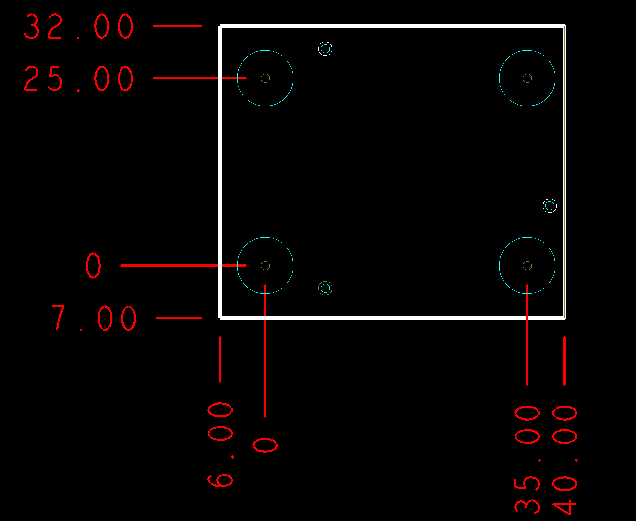
Image credit: Author - Datum dimensions based on the board origin
An example that comes to mind is where there is a slot in the board that is designated for a nice tight fit with a mating connector. The tolerance from our origin allows the near edge to be anywhere within the standard tolerance, say +/-0.1 mm. The far edge also has the same allowance based on the common datum. This is called a tolerance stack-up, and it allows twice as much slop as a linear dimension of the slots two edges.
Labeling (the dimension) for First Article Inspection (FAI) ensures that the measurement is taken and recorded when introducing the initial run of the product.
If the width of the slot is a defining feature, a dimension from one slot edge to the other will be more useful. Labeling it for First Article Inspection (FAI) ensures that the measurement is taken and recorded when introducing the initial run of the product.
Datum, or direct, the geometry is captured either way. The CNC machine that cuts out the board outline isn’t capable of distinguishing anything other than the nominal values. It does not care how you dimensioned anything. It is already doing the best it will do given the CAD data. The care put into the dimensions and the drawings will be used at the end of the line by an inspector to determine whether to accept or reject an entire lot of boards. Giving that person a heads-up on the requirements is the point of the whole document. Showing them exactly what to measure helps ensure execution through the higher level assembly processes.

Image credit: author - using trailing zeros to indicate precision.
Just Follow the Recipe?
Unfortunately, we often find ourselves in the middle of a conflict between our vendors. The issue centers around the component vendors with a penchant for utopian datasheets. To be competitive, they have to put a lot of things into a small space. To have confidence that their product will not be the weak link, they become very conservative in their approach to the recommended footprint. While these highly engineered footprints provide near 100% confidence that the part will fit, the PCB fabricator lives in the real world and would appreciate a little extra wiggle room in the spec.

Image credit: Author - How many design rules can we break with one connector?
The notorious USB 3 Type C connector provides plenty of obstacles for the fab shop. The co-mingling non-plated holes and slots with plated holes and slots and SMD pads are bad enough. Then, so many features are hugging the board edge; this is a classic case of the component vendor overshooting the PCB factory capability.
To be clear, there is enough vertical integration of the PCB industry that your vendor likely has more than one location, each with varying degrees of technology. Talking you down to the lower cost or under-used shop is part of their ongoing plan. Chances are that they can do the job to the datasheet constraints but only in their upper tier factory. That gleaming showpiece is for someone else’s boards.
Bringing the board and part suppliers together to hammer out a compromise might help. Most of the vendors that have been asked for spec relief stand by their doc as the only way they will warrant their product against failure. It puts you in a tough space with your fabricator, but you may have to pony up if you want to use the technology that everyone else is also chasing.
Unilateral/unequal tolerances
It’s not unusual for the part supplier to recommend a slot that has a limit dimension; an upper and lower figure with acceptance falling anywhere between. Another trick is to have a minimum size stated as the working number with a positive tolerance but no negative tolerance. Shameful! A normal distribution curve of a process in control has the shape of a bell. The call-out makes it look like we want a half of a bell curve where the majority of the measured values hit the upper limit, but none go over.
The best dimensions give a nominal value and equal tolerances on either side.
The world doesn’t work that way. I’ve studied this stuff while running a receiving inspection lab and over the years since then. The best dimensions give a nominal value and equal tolerances on either side. Limit dimensions that provide the upper and lower boundary are useable, but they leave it to the designer to come up with a nominal value for the affected features.
3 Sigma
There will be times when the “secret sauce” of the project pushes the boundaries of what normal factories produce. The tricky part of the operation comes under scrutiny that does not let up until the yields are under control. If the process window for an attribute requires an extra tight range and cannot be opened further, then the tolerances should be established around the hard-stop limits. You do what you have to do and pay that price.
Meanwhile, you’re back at the lab working out a better plan with the team. If something we designed turned risky or a costly beyond our comfort zone, our goal shifts to a new and improved version that has a chance of making us some money. Go back to the factory with something that has a 99.7% success rate or better before calling it a day. Factory defects will put a dent in a program. Unchecked defects will sink a company. Properly defining a design will help you stay away from those costly defects.