Managing High-Density Vias
Key Takeaways
-
The case for high-density interconnect PCB designs
-
The vias used in HDI designs
-
Effective via management using design constraints
Vias in a printed circuit board being examined under a microscope
Most people are familiar with going into a hardware store for everything from cleaners to light bulbs, but have you ever noticed all of the different types of mounting hardware they carry? There are nails, screws, nuts, and bolts to start with, and then those are then broken up into wood, metal, galvanized, plastic, or finishing. Next, they are subdivided by metric or standard, and then sorted by their length, width, and thread pitch. How these stores keep all of this inventory managed is beyond me.
Thankfully in the world of PCB design, we don’t have nearly that many different items to keep track of. There are, however, a lot of design objects like vias that do need managing, especially in a high-density design. While older designs may have used only a few different vias, today’s high density interconnect (HDI) designs require many different types and sizes. Each of these vias needs to be managed [link to Constraint Usage for Management] in order for it to be used correctly to ensure maximum board performance and error-free manufacturability. Let’s take a closer look at the need for managing high-density vias in PCB design and how this can be done.
Considerations Driving High-Density Printed Circuit Board Designs
As the demand for smaller electronic devices escalates, the printed circuit boards that drive them have had to shrink along with them in order to fit in the box. At the same time, electronics have had to respond to the call for increased capabilities by adding more components and circuitry to the board. To further complicate the problem, PCB component sizes keep decreasing while their pin-counts grow in number, forcing the use of smaller pins with tighter pitches. For the PCB designer, the bag kept getting smaller while everything that went into the bag got larger, and soon the traditional methods of circuit board design had reached their limits.
In order to accommodate the need for increased circuitry on smaller board sizes, a new method of PCB design was introduced known as high density interconnect, or HDI. These designs make use of newer fabrication techniques to build boards with smaller line widths and thinner materials, as well as blind and buried vias or laser-drilled microvias. Together these high-density characteristics enable more circuitry to be manufactured in a smaller area of the board and provide a viable connection solution for large pin-count ICs.
The use of these high-density vias also yields a couple of other benefits:
-
Routing channels: Since blind and buried vias as well as microvias do not go all the way through the board layer stackup, this opens up additional routing channels in the design. Through the strategic placement of these different vias, the designer can now route out of parts that have hundreds of pins on them. Components with this many pins would normally choke off all the inner layer routing channels if only the standard thru-hole vias were used.
-
Signal integrity: Many of the signals on these devices also have specific signal integrity requirements that can be jeopardized by the full length of a thru-hole via barrel. These vias can act as antennas radiating EMI, or affect the signal return path of a critical net. Using blind and buried vias, or microvias however, eliminates the signal integrity problems that could be caused by the extra length of a thru-hole via.
To get a better idea of the vias that we are talking about, we’ll look next at the different types and applications of vias that can be used in a high-density design.
The via list in PCB design tool showing the types and configurations of different vias
High-Density Interconnect Via Types and Structures
Vias are holes in a circuit board connecting two or more layers in the stackup. Typically the via conducts a signal traveling on a trace from one layer of the board to its corresponding trace on a different layer. To conduct the signal between the trace layers, the via is plated with metal during the fabrication process. Vias will come with different-sized holes and metal pads depending on what they are used for. Smaller vias are used for signal routing while larger vias are used for power and ground routing, or to help provide relief for components that run hot.
Here are the different types of vias that you will see in use on a circuit board:
-
Thru-hole: A thru-hole via is the standard via that has been in use since double-sided printed circuit boards were first introduced. The hole is mechanically drilled through the entire board and plated through. Mechanical drills do, however, have limitations on how small they can drill, which is dependent on the aspect ratio of the drill diameter compared to the thickness of the board. Typically a thru-hole via can not be reliably drilled or plated any smaller than 0.15 millimeters, or 0.006 inches.
-
Blind: This via is also mechanically drilled just like a thru-hole via is, but uses additional fabrication steps to drill only through part of the board layers from the surface. These vias also have the same drill size limitations as thru-hole vias do, but they do allow for additional routing channels above or below them depending on the side of the board they are on.
-
Buried: Like a blind via, a buried via is mechanically drilled but starts and stops on internal layers of the board instead of coming from a surface layer. This via also requires additional fabrication steps due to being buried within the board layer stackup.
-
Microvia: This via is drilled with a laser in order to create a hole that is smaller than the 0.15 millimeter limitation of a mechanical drill. Since a microvia will only span two adjacent layers of the board, its aspect ratio allows for a much smaller hole for plating. It can also be placed either on the board surface layers or internally. A microvia is often filled and plated so that they are essentially hidden, which allows them to be placed in a surface mount component pad for parts like a ball grid array (BGA). Due to its small drill size, a microvia also requires a much smaller pad than a regular via, around the size of 0.300 millimeters or 0.012 inches.
A diagram of a typical microvia used in a high-density design
These different via types can also be configured to work together in different patterns depending on the needs of the design. For example, microvias can be stacked together with other microvias, or they can be stacked together with buried vias. These vias can also be arranged in a staggered pattern with each other as well. And as mentioned earlier, microvias can be used within the pads of surface mount component pins. This further eases trace routing congestion by eliminating the traditional trace routing from a surface-mount technology (SMT) pad out to an escape via.
Those are the different types of vias that can be used in an HDI design. Next, we’ll look at how PCB designers can best manage their use.
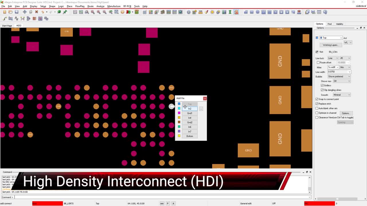
Managing High-Density Vias in PCB Design CAD Tools
Although there are only a few types of vias that can be used in a PCB design, there is no end to the ways that different via sizes and shapes can be created. Power and ground connections will typically use a larger thru-hole via than what is used for regular routing, except for the bottom side of large BGA parts that have several hundred pins in them. For those, a microvia in the surface mount pad will probably be necessary along with the other BGA pads. And while some of these larger parts will benefit from the use of microvias, the regular surface mount parts with fewer pins won’t, and a standard thru-hole via can be used for their routing. These thru-hole vias will be smaller than the power and ground vias, while thru-hole vias used for thermal dissipation will be even larger yet. Then there are all of the different sized blind and buried vias that can be used.
Needless to say, on an HDI design there can be dozens and dozens of different vias necessary to fulfill all of the design requirements, which can get a little confusing. While a designer could possibly keep track of several of these, the vias become more and more difficult to manage as the number of different sizes grows. Not only does the designer have to track all of these vias, but different vias can be used on the same net depending on the area of the board being used. A clock signal, for instance, may use a microvia in an SMT pad to route out of a BGA pin, but then revert to a buried via further down the line. But you wouldn’t want to use a thru-hole via for this net because the extra length of the via barrel could create an unwanted antenna on that line.
Obviously, a better solution for via management is needed. Fortunately, PCB design CAD system innovators like Cadence have already provided the tools that designers need to properly manage their high-density vias.
The constraint management system in Allegro PCB Designer being used to manage via clearances
Using an Advanced Constraint Management System
By using the Constraint Manager in Cadence’s Allegro PCB Designer, each net can be assigned one or more vias to be used while trace routing. This will take the pressure off the designer to manually filter through all the available vias when connecting each net. Net classes can also be set up for groups of nets, and these classes can be assigned specific vias making their management that much simpler. Additionally, multiple via constraints such as spacing can be assigned to vias globally, or to specific layers and regions of the board. You can also assign spacing constraints to the different via types that you are working with as you can see in the picture above.
Using the constraint management system in Allegro PCB Editor will greatly simplify the task of managing high-density vias in your HDI PCB design. For more information, take a look at our E-book on high-speed designs.
If you’re looking to learn more about how Cadence has the solution for you, talk to us and our team of experts.