The Best PCB Via Size Guidelines for Your Design
Key Takeaways
-
How does via type affect via size?
-
What are the restrictions on PCB via size?
-
How to optimize via size on your board?
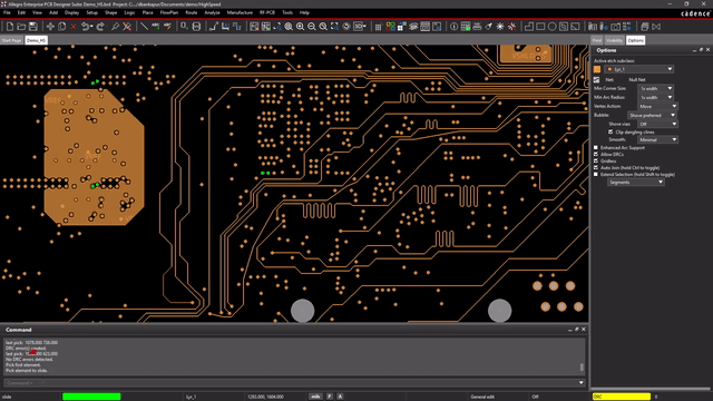
PCB with different size vias
While some of us may believe in the “bigger is better” philosophy, one area where smaller or more compact is often preferred is PCBA development. The trends toward smaller circuit boards--and electronics products in general--over recent decades is undeniable. The challenge in achieving this objective has been how to improve or enhance functionality and capability while simultaneously reducing board size. There have been a number of technological advancements that have made these changes possible, including more compact components, thinner on-board traces, and higher density interconnect (HDI) connectors.
However, the most important reason that the demand for smaller boards is able to be met is the increase in the use of multiple-layer stackups and vias. Vias come in various sizes and have different applications on circuit boards. They can be both underused and overused, and designers must find the proper balance for their design. A good start is to understand how much space vias should occupy and follow a set of PCB via size guidelines to help you decide where and when to utilize this asset.
Via Type vs. Via Size
Although vias are typically round and proceed vertically through the board structure—as opposed to horizontally, as copper traces do in most cases—they have the same objective. That is to aptly carry the current capacity required between components or other PCBA elements. This is true for all of the via types shown below, except when the via is tented or closed.
Various via options. Image source
As shown above, all of the via options originate and terminate in a pad, which separates vias from other drill holes. From the figure, we see that vias may be open or closed, which means their purpose may be to carry signals, current, or heat or to prevent current flow.
The fact that vias have different functions plays a role in how their size or diameter should be determined, as listed below.
The guidelines above should inform your PCB via size determinations in order for the via to meet its performance requirements; however, there are other considerations that should be addressed.
Additional PCB Via Size Guidelines
As with other choices for your circuit board design, your choice of via type and size should not be made without considering the impact on other aspects of your design and development process. For example, manufacturability should always be a major concern, as even the greatest design is useless unless it can be built. The list below provides essential issues that should be incorporated into your PCB via selection process.
Considerations for PCB Via Size Selection
- Board classification
Prior to selecting a via size, the board classification needs to be determined, based on the board’s component density as follows: - Level A - Low density and general design productibility.
- Level B - Moderate density and design productibility.
- Level C - High density and design productibility.
- Fabricator equipment capabilities
Although most manufacturers have a robust range of drill hole sizes that they can produce, it is critical that you work with a CM that has the capability to produce the size vias that your design requires. - Board density
In addition to affecting your board’s classification, the density of components and other elements directly impact the clearance requirements and, consequently, the size of your stackup and the number of vias needed to meet operational objectives. Inadequate clearances and ill-designed stackups can significantly increase the EMI on your board, which degrades signal integrity. - Via density
Many boards, especially if comprised of high pin count SMT ICs, can have significant numbers of vias. Coupled with high-power requirements and the need for thermal vias, this can lead to high via density, as shown in the figure below. Care must be exercised here, as this may affect board parameters such as impedance and structural integrity.
3D image of high via density
Selecting PCB via size is not an isolated task; instead, you should consider its implications on other design parameters and manufacturability. With this perspective, a set of good PCB via size guidelines, and the proper PCB design package, you can optimize your board layout.
Making the Best Use of Vias for Your Design
Most vias are round or circular, however, component pads to which they connect may take on other shapes, as shown in the figure below.
Cadence PCB Design Software Padstack Editor
For pads that carry current, the geometry is important in determining the signal’s electrical parameters as well as the size of the via, similar to surface traces and pins. Therefore, it is important that you utilize a PCB design package that includes comprehensive via management functionality. This includes various sizes, the ability to implement via constraints, and advanced routing capabilities as available with Cadence’s Allegro PCB Editor. Armed with the right tools and design approach, the following PCB via size guidelines can be readily implemented.
How to Optimize Your Via Size Selections
- Understand the current carrying requirements for your traces
For current carrying vias--signal, power, and ground--it is important that vias are able to transfer the signals with high-fidelity, minimal loss, and within ampacity limits. - Use effective trace width and spacing tips
Routing surface traces and vias are not separate activities. In fact, a primary purpose of vias is to complete circuits between surface components. Therefore, the more effective your trace routing and spacing, the better your via selection and utilization should be. - Adhere to IPC-2222 standards for minimum hole sizes
Once your component density classification has been determined, you should use the following equations to comply with the IPC-2222 Standard for minimum hole size.
Level A Minimum Hole Size = maximum lead diameter + 0.25 mm (1)
Level B Minimum Hole Size = maximum lead diameter + 0.20 mm (2)
Level C Minimum Hole Size = maximum lead diameter + 0.25 mm (3)
- Determine the pad sizes based on IPC-2221
After determining minimum hole size, Eqs. (4 - 6) from the IPC-2221 Standard should be used to determine pad diameter.
Level A Pad Diameter = minimum hole size + 0.1 mm + 0.60 mm (4)
Level A Pad Diameter = minimum hole size + 0.1 mm + 0.50 mm (5)
Level A Pad Diameter = minimum hole size + 0.1 mm + 0.40 mm (6)
- Minimize the number of vias required
Another good rule of thumb is to tend toward less via usage as opposed to more. Over usage may have implications for board mechanical and electrical properties. - Collaborate with your CM for the range of via sizes that can be drilled
For the most efficient board manufacturing, you should always work with the CM that will actually build your board. This is also true for via selection, as drill hole capabilities may vary from manufacturer to manufacturer, especially with respect to aspect ratio limitations and minimum hole size.
Properly selecting via type and size is important for creating good designs that optimize space and meet performance objectives. However, effective routing requires an understanding of the relationship between surface routing and routing to and through planes, which you can get by reading this E-book.
Leading electronics providers rely on Cadence products to optimize power, space, and energy needs for a wide variety of market applications. To learn more about our innovative solutions, subscribe to our newsletter or our YouTube channel.