Uncovering PCB Embedded Components
Key Takeaways
-
The benefits of using PCB embedded components.
-
How these parts are fabricated into a circuit board.
-
Design considerations and setups for using PCB embedded components.
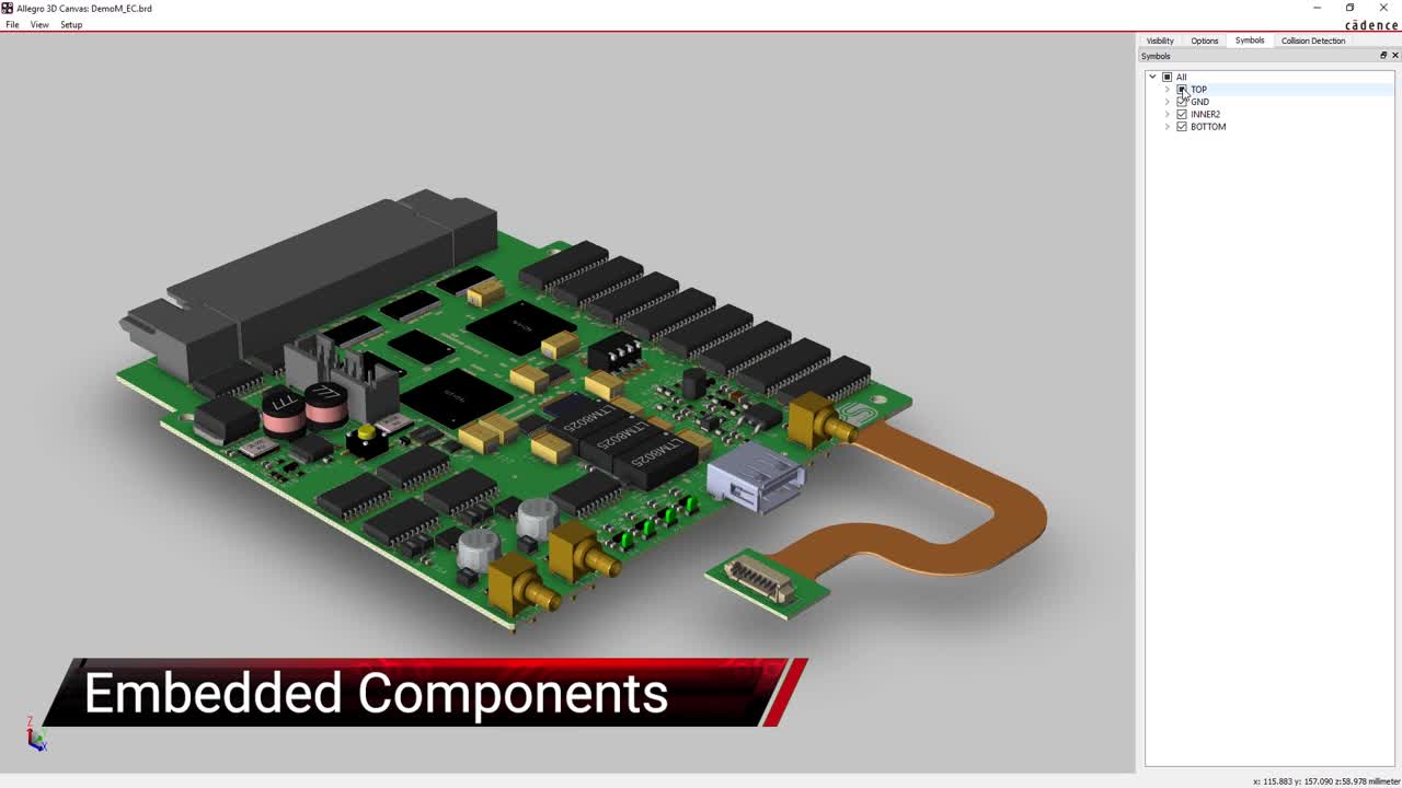
A CAD view of PCB embedded components
Circuit boards started as a simple substrate with holes for component leads to go through. These leads could then be soldered to wires to complete the circuits. Conductive paths, or traces, were then added to the substrate to remove the need for soldering wires, and, before long, components were being soldered to both sides of the board. Thru-hole parts led to surface mount parts, which got smaller and smaller while their pin counts and densities increased. This progression naturally led to the question, “What will the next advancement in printed circuit board technology be?” The answer is PCB embedded components.
The concept of embedding components into the substrate of a circuit board has been around for a long time now. What is new is the technology to mass-produce circuit boards with embedded components and the market requirements driving designers to use these parts. This article will look at PCB embedded component technology and how you can use it in your own circuit board designs.
What Are the Benefits of Using PCB Embedded Components?
Using PCB embedded component technology can be very useful in some circuit board designs. Here are some of the benefits that these parts have to offer.
Miniaturization
Embedded components are used in both rigid and flex designs. By reducing the number of components that have to be installed on surface layers, embedded parts can reduce the overall size of the circuit board. Or, depending on your needs, embedded components can help you fit more parts onto the same size board. For instance, terminating resistors that are typically placed next to or on the opposite side of a large pin-count BGA can be embedded directly beneath the part.
Electrical Performance
With the ability to place parts inline to the signal path directly under their connecting parts, the connection paths between the two can be reduced in length, improving signal integrity. Shorter connection lengths will reduce parasitic effects in high-frequency circuits and decrease the capacitance and inductance within the power delivery network that creates noise. Additionally, EMI shielding becomes much easier by simply surrounding an embedded component with thru-hole ground vias.
Mechanical Reliability
By embedding components that used to be soldered onto the surface layers, there are fewer solder connections that can fail, thereby improving the mechanical reliability of the board. Thermal management of embedded parts is also easier to achieve with the ability to put the part into direct contact with thermal microvias to dissipate heat.
Cost
Using embedded components instead of surface mount or thru-hole parts will reduce the amount of assembly required for the board. This can be a cost-saver, especially for complex high-density boards that require intricate manual assembly to fit all of their parts together.
However, there are a couple of negative aspects of embedded components to be aware of:
- Embedded components can be affected by the normal soldering processes the board will go through during PCB assembly.
- Embedded components can not easily be tested after manufacturing.
- Embedded components can not be easily replaced in the case of retrofitting the board or repairing it.
So, how are PCB embedded components manufactured into a board? We’ll look at that next.
Placing an embedded component in a design using the place on layer option within a PCB CAD system
How Are Components Embedded in a Printed Circuit Board?
Both passive and active components can be embedded in a circuit board using one of two processes:
- Placing components within interior cavities created in the circuit board.
- Molding components into the substrate.
The cavities needed for placing embedded components within the board structure can be formed with different production techniques. One such method is drilling the cavity with a laser to remove dielectric materials to a precise depth. Once the cavity has been created, a conductive adhesive material is added to hold the part in the cavity. This conductive adhesive will melt with applied heat and form a good solder bond to the part, similar to solder paste. Cavities can also be created with small milling and routing tools, but are size restricted due to the physical size and shape of the equipment. Some thin wafers can also be fabricated directly into the board’s dielectric materials, bypassing the need for drilling or routing a cavity. These parts are embedded into the board during the lamination process.
Here are some more detailed specifics on embedding various parts:
- Passives: Most passive parts are now formed into a circuit board using different values of conductive ink, copper foil, and dielectric materials. These parts must be designed into the board during layout, and require the designer to specify the exact materials necessary for each embedded component. Resistor materials can be either printed onto the resistor pattern in the board or created using sheets of thin-film resistive material. Capacitors are created by laminating dielectric material between the embedded part’s copper conductors or screen printing the dielectric material onto the component’s pattern. An inductor’s spiral or bending shape is created by etching the copper or plating the copper up.
- Actives: Semiconductors are usually embedded in a cavity. Designers must be careful to line up the die bonds for the most direct connections between the embedded part and the external part it is connecting to. There are different methods of manufacturing an embedded integrated circuit. In some cases, the cavity is filled with a polymer material to mold the chip to the substrate. In other cases, the chip is pre-installed onto materials for incorporation into the circuit board.
As you can imagine, working with embedded components takes a lot of care on the part of the designer. Placement tolerances must be obeyed, and we will look more into that next.
This cross-section editor also gives intuitive tips on the configuration of the cavity design rules
Design Considerations When Working With Embedded Components
When working with PCB embedded components in a layout, designers will want to be mindful of the regular aspects of placing and routing a component on a circuit board. These considerations include positioning the components for the shortest connection paths and the most optimum rotation of the part for routing. However, in addition to place and route, there are two other details that need the attention of designers: materials and cavities.
Materials
It is essential to choose the correct materials for the embedded components in a PCB design. For passive components like resistors, the materials will ultimately determine the value of the part. Capacitors will require the appropriate dielectric material to be used between carefully designed copper plates. When embedding active components, the choice of materials for filling the cavities is critical to the long-term reliability of the embedded ICs being used. To avoid manufacturing failures of circuit boards with embedded parts, designers must choose component and substrate materials that are compatible with each other.
Cavities
Designers must consider the size of their components in order to create the correct cavities that align with the DFM rules of the board. Usually, these values are controlled by PCB CAD systems such as Cadence’s Allegro PCB Editor within their Cross Section Editor, as shown in the picture above. Designers also must choose between facing the components up or down within the cavities. Facing them down gives better control over the dielectric’s thickness and placement accuracy.
Now, we’ll see how designers can set up some of these values within a PCB CAD system.
Allegro’s Constraint Manager will allow the designer to configure embedded components with design rules
Setting Up Allegro X for PCB Embedded Components
In Allegro X, there are two main tools for setting up the constraints for working with PCB embedded components. The Cross Section Editor gives the designer control over what layers can be used for embedded components. It also provides the mechanism for setting up spacing constraints for the size of the cavity and its proximity to other cavities.
The second utility that a designer will need to configure is the Constraint Manager. This tool facilitates configuring each individual component, or classes of components, with their embedded rules and constraints. With this tool, you have the option of setting up the components to be placed on external or internal layers, or both. No matter what configuration you need for your embedded components, Allegro X can give you the features and functionality you need for your design.
If you’re looking to learn more about how Cadence has the solution for you, talk to our team of experts.