Winning With Fewer PCBs
The business world keeps score with dollars and cents. The overhead cost of layout and material cost of bare boards are a significant drain on capital. Face it; Printed Circuit Boards are expensive. The value that a Designer can add is to reduce the overall cost of boards. If not for that, the enterprise could put a CAD license on anyone’s desk and let them have at it. Just imagine if CAD tools were easy to use! That day may come so we are well advised to find other ways to earn our keep.
“One job featured a flexible circuit called “the Hydra” on account of the various connectors forming a serpentine hairdo for the central rigid section.”
Giving educated advice on system architecture is one possible avenue. We know the boards, the parts, the connections and enough about the hardware to be an asset to the Physical Design. The layout function has unique insights on how a flex circuit can be as simple as a ribbon cable or as complex as a vehicle’s entire wiring harness. The depth, breadth, and value of PCB design is what you make of it. Some of that knowledge can contribute to the overall picture in terms of the number of PCBs in a system.
Things to consider when combining boards:
-
Complexity - matching the technology in terms of stack-up and architecture
-
Power - similar voltages and noise floors
-
Edge rates, resonant frequencies - victim vs. aggressor traces coexisting.
-
System wide connections - are the endpoints in similar locations for a flexible solution.
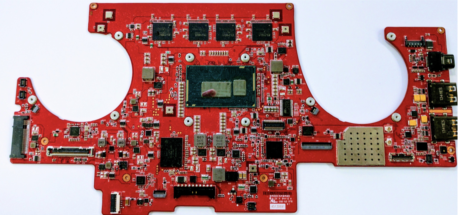
Image credit: Author - can you find the 15 edge connectors?
Chromebooks For The Win
Designing the PCBs for Chromebooks was my main occupation for years, so I’m comfortable using laptops as an example. The trick with laptops is that so much is happening on the screen side of the hinge. All of that information needs a wide pipeline to the keyboard side. Beyond the display itself, we also have a camera module, RF antennas and maybe even a row of colored LEDs for decoration. Power and data have to squeeze through the hinge for all of those things. Their locations are hardwired, but a long, skinny circuit across the top could incorporate cameras, microphones, printed antennas and various sensors.

Image credit: Author - a bit of work went into the row of lights on the case.
Under the keyboard, there may be a few opportunities for unification. Assembly and serviceability are the primary concerns at the end of the line. In the meantime, getting the heat out is the engineering challenge. The bare minimum Main Logic Board (MLB) has the System On Chip, (SOC) external memory, the Power Management Integrated Circuit (PMIC) and connectors. A plethora, make that two plethoras and one bevy of connectors that mostly connect to bespoke flex circuits. A lot of meetings took place regarding the optimum topology for this product.
Keyboards, trackpads, and batteries have standard connectors, but the path from the unit to the MLB aka “motherboard” varies, and so does the standard cabling lengths. The other goodies usually require custom flex circuits. This is where you need to get creative.
One job featured a flexible circuit called “the Hydra” on account of the various connectors forming a serpentine hairdo for the central rigid section. Another one had an acronym, tROtS for “the Rest Of the Story”. The ROS board was the catch-all for the functions that didn’t make it onto the main PCBs of the system. It does not have to be an all-in-one solution to help. A two-in-one strategy employed in a couple of places puts the math in your favor as well. Turning 12 boards into 10 is a win.
Pile On
Looking back at the MLB, a fair number of functions were brought on board including WIFI (under the can) and the audio just to the right by the lower USB 2 connector. That little chip drove this board from a 1+N+1 stack-up construction to a 2+N+2 which was a cost hit. It was also a relief that the extra layer of micro-vias improved the DDR routing to those four devices at the top of the board. Fun stuff when you add a 0.4 mm pitch BGA to the mix. Ideally, any new parts will not drive the PCB to a higher technology level. Trade-offs are a part of the game.

Image credit Christopher Ross - Fully loaded with batteries, speakers and heat spreaders.
The board itself was essentially poured into the space between the fans and the lower chassis. The back side has headroom for the very smallest parts only. Many of the sensors as well as the NFC are on-board while the GPS and microphone array are on their own flex or boards. Our goal was to get as much on this 10-layer board as possible.
A lot of what looks like open space is reserved for things like the heat pipe and cabling. That Intel SOC radiates big time, so we went all in to make a cool Pixel with all of that power. I’d say it worked out pretty well as Google products go. It received solid to glowing reviews and few actual buyers. Other Chromebooks did the heavy lifting on the raw numbers side. I see this same thing playing out with the Pixel phone too. Samsung and others will continue to make the Android phones and Chromebooks while Google makes (M)ad-money on its core business.
The Wrap
Whether your business is small or large, the benefit of a reduced Bill of Material is undeniable. Simplifying labor and increasing reliability are two side benefits. The main cost is in up-front engineering. It’s expensive to create a solution that is acceptable in both coexistence and functionality. Someone who has been down in the trenches between the traces can really be beneficial to the Industrial Design and/or Product Design teams. Put those insights to good use to help your company’s bottom line and expand your toolkit.