RC Snubbers and RCD Clamps for Isolated DC-DC Converters
Take a look at reference designs for isolated DC/DC converters, such as flyback converters or push-pull converters. These power supplies take advantage of magnetic coupling to transfer power from an input to an output and thereby step up or step down voltage. In the process of doing so, these circuits generate multiple types of switching noise which can be seen as conducted or radiated emissions. The switching noise can also be resonant, which creates large current spikes in certain components.
The way to deal with these current spikes is to clamp the voltage or use snubbers. Snubbers and clamps in isolated switching converters are sometimes referred to interchangeably because they perform similar functions. They can also be used at the same time, although traditionally you will only find one of these elements at any given time. Let's look at both types of circuits to see how they can be used to damp certain switching noises in switching converters.
Which Noises Do Snubbers and Clamps Suppress?
RCD clamps and RC snubbers are used to dampen or suppress noise produced by switching signals that interact with leakage inductance in transformers. The image below shows placement of a transformer and clamp in a flyback converter. Note that many guidelines will call this circuit a snubber, but other guidelines will call a series RC circuit a snubber.
Flyback converter with parasitics and clamp/snubber circuits. (Modified from image source)
Noise from the leakage inductance is excited on the downward edge of the switching signal driven into the transformer coil. When the driving signal switches from high to low, that drives a forward voltage that forward biases the diode in the circuit above. This current loop passes through the leakage inductance and parallel drain-source capacitance in the switching MOSFET.
When a series RC snubber circuit is used instead of the clamp circuit, the RC circuit can provide damping on the rising and falling edges because there is no diode to bias during either transition.
RC Snubber Calculation
Sizing of the RC snubber requires knowledge of a ringing waveform at the switch node, which is normally obtained through measurement. An RC snubber can be placed on the primary side or the secondary side, although it is most common to see an RC snubber on the secondary side. Still, it could be placed on the primary side in addition to an RCD clamp. To design the circuit, the following must be measured:
-
The coil’s leakage inductance
-
The ringing period without the RC snubber
Using a measurement of the period of the ringing waveform (T), this can be used to calculate the required RC time constant.
Based on this value, the required R and C values can be calculated. To get the resistor value, the simplest approach is to set the resistor equal to the impedance associated with the transformer’s leakage inductance.
With these two equations and the measurements of T and L (leakage inductance), we now have the component values for the RC snubber. Some adjustments typically need to be made to account for power dissipation or residual ringing in the number.
RCD Clamp Calculation
The RCD clamp circuit is also designed by accounting for leakage inductance that is present on the connection to the switching node. However, because the leakage inductance is present on the switch node, it also interacts with the drain-source capacitance of the switching mosfet. Together, the leakage inductance and output capacitance create an underdamped oscillation during the falling edge of the switching waveform. This is show as the Vclamp waveform below.
The role of the RCD clamp is to absorb the energy released by the leakage inductance. The power delivered to the snubber circuit by the underdamped oscillation is equal to:
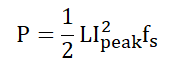
Here, I(peak) is the maximum drain current immediately before the MOSFET turns off. Next, we can calculate the clamp resistor value based on the allowed voltage across the snubber (note: Vs = Vclamp and nVo = Vfly in the above waveform):
Finally, the capacitor can be calculated by accounting for the variation in the clamp voltage. As can be seen, a larger resistor and a larger capacitor will reduce the ripple in the clamp voltage:
If the leakage inductance is not known, then measurements of the clamp voltage could be used to determine what is the leakage inductance. Another approach is to use reasonable estimates of leakage inductance and adjust the circuit parameters by swapping components. From these two approaches, you can determine the optimal circuit values in a prototype and later verify these in simulation or measurement. A low-cost LCR meter can give a very good measure of the leakage inductance.
Whether you need to design large power electronics or compact high-speed digital PCBs, use the complete set of circuit simulation features in PSpice from Cadence. PSpice users can access a powerful SPICE simulator as well as specialty design capabilities like model creation, graphing and analysis tools, and much more.
Subscribe to our newsletter for the latest updates. If you’re looking to learn more about how Cadence has the solution for you, talk to our team of experts.