Working with Ball Grid Arrays or... Why I see Spots All the Time
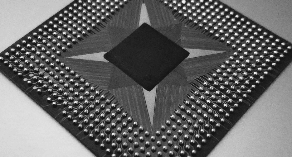 You cannot get away from these things. (My photo, Aperto Networks FPGA)
The little four-pin FETs (that give everyone fits!) on up to the system on a chip, it is getting harder and harder to find a product without some BGAs on board. So let's jump in with both feet.
History
They have been in use for a few decades with no signs of slowing down. They are a surface-mount descendant of Pin Grid Arrays. Before their adoption, the most common form of higher density packaging was the Quad Flat Pack (QFP) where the leads broke out on all four sides. Those devices, in turn, supplanted the two-sided lead frames of the Small Outline Integrated Circuit (SOIC) and the venerable Dual In-line Package (DIP) that got us to the moon and back.
Solutions lead to problems ad infinitum.
Each generation came about for the same reason. More stuff was going on under the hood of the chips. We needed more connections from the die to the outside world. Essentially, Moore's Law drove us to the point where the linear space around the package was no longer sufficient for all of the I/Os. 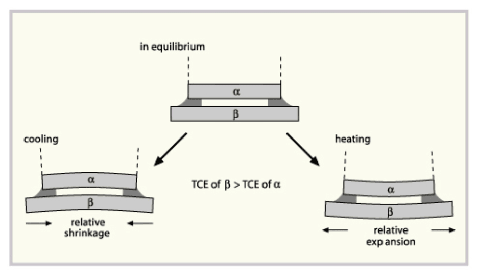
Diagram credit: Ceramic Metal Bonding Technical Group.
The leads on those first components served an essential purpose aside from being a conduit for the signals. As we know, matter expands and contracts with temperature fluctuations. Hot things grow - and glow in the infrared part of the spectrum. The rate at which different materials expand and contract varies. The rate of change is known as the Coefficient of Thermal Expansion or CTE. The variance of the rates of different materials gives us the CTE "mismatch," and that is the thing we solve by giving our components little legs on which to stand.
The material of the substrate and the die itself had a CTE that was closely matched. Why? Because otherwise, a failure from thermal cycling the die and its carrier would be a problem owned the chip house. Can't have that. Pushing the omnipresent failure mode over to the system made good sense and saved many cents for the chip vendors. The go-between was in the shape of the leads. Gullwing or J-lead and other configurations provided a natural stress relief as the parts warmed up ahead of the printed circuit board.
Metal fatigue is real and presented a real problem for the early designs -- still does. Back in the day, somebody showed me how to break a wire clothes hanger just by bending it back and forth until it failed. There's no other way an 8-year-old kid could rip that hanger apart with their bare hands. Lessons learned. Don't thermal cycle things to their breaking point.
The rubber meets the road at the tiny ball of solder that gives the BGA its name.
Solving this problem fell on the material scientists of the day. If you have ever seen a Chip On Board (COB) you will notice the thing is covered by a hard cocoon; what's known as a glob-top. Its obvious apparent is to protect the tiny chip. Less obvious is to prevent the underlying board from expanding and contracting at its regular rate. The glob tenaciously holds the surrounding PCB material so that the solder joints do not rip apart when the board tries to grow or shrink faster than the device. Continuing work at both ends brought forth substrate and PCB materials that could coexist as temperatures rose and fell.
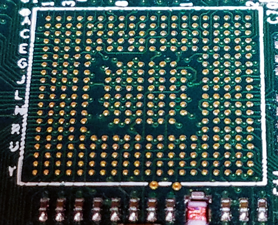
My photo, Airgo Networks baseband chip (unpopulated)
Ceramic is more stable under temperature loads caused by the chip heating up while doing its many jobs. Plastic is elastic and makes a good commercial grade choice for the material between the die and the board. The rubber meets the road at the tiny ball of solder that gives the BGA its name. Making the balls out of a soft metal with excellent pliability and quick transitions from liquid to solid is an ideal solution. A relatively low melting/freezing point will also help. The best alloy ever found is one of 63% tin and 37% lead. It is known as eutectic solder. This nearly perfect solution has that one flaw. Lead. It is a silent killer and is mostly banned.
So far, the replacements have a much higher melting point and are quite a bit stiffer once they solidify. We feel the pain twice. Once when we attach the device to the board, and again (and again) every time we flip the switch. Once we achieve the perfect the soldering profile, non-trivial in itself, we are left with brittle solder joints that are prone to cracking. The latent defects caused by this phenomena are the worst because the product works – until it does not.
The latent defects caused by this phenomena are the worst because the product works – until it does not.
Problems lead us to solutions. The same idea of glob-topping the chip-on-board is used another way. Instead of encapsulating the whole shebang, we use an underfill material that creeps into the crevasses under the BGA and holds everything in place once it cures. Underfill is apart from the so-called conformal coating that NASA sprays over the entire PCB assembly. Both of these processes make rework all but impossible. Solutions lead to problems ad infinitum.
Keeping it Cool
Pictured here is an illustration from our friends at Intel that depicts a flip chip on a BGA substrate. The thermal path is downward through the bumps and the substrate to the solder balls and eventually into the PCB itself.
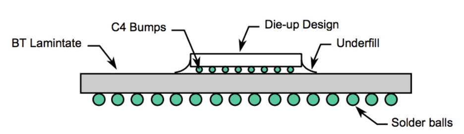
Diagram credit: Intel
The other approach is a cavity down set-up where we employ a heat sink, a tiny fan or heat spreader to the top of the component. This is quite robust and capable of dissipating the many watts that are needed to run our super-computing devices. Thermal energy is still transferred to the board but is not the main path.
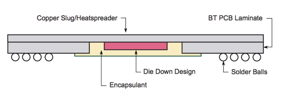
Diagram credit: Intel
Circling back to Gordon Moore and his overachieving lawyers, density continues unabated. Once upon a time, the standard pin pitch of the BGA balls would be 1/20 of an inch. In metric terms, that is 1.27 millimeters. We have stepped down to 1.0 mm then to 0.8 mm down to 0.65 mm which is the smallest pitch that has any through-hole routing solution. Even though that's dodgy, and we weren't done.
Honey, I Shrunk the Chips!
Around the turn of the century, High-Density Interconnect (HDI) trickled down from the cell phone industry (as far as I can tell) and enabled BGAs to reduce the pitch down to 0.5 mm. Micro-via-in-pad is the only reasonable way to handle the fan-out at this pitch. I was on board with a device that managed chromatic dispersion for the optical data transmission sector. Getting vendors who could scale it up was problematic for a start-up when all of the big boys were hogging the HDI supply chain.
It has gotten easier. More and more PCB vendors have joined the fray. China has the majority of factories that deal with the 0.5 mm and 0.4 mm pitch devices. For me, it was Qualcomm that ushered in the era of the 0.4 mm parts. Not content with even rows of balls, we used an offset pattern that allowed even tighter integration. Instead of four equidistant neighboring pins, we wrestled with six adjacent pins in a honeycomb pattern. Mayhem!
They had me doing reference designs for a supplier who wanted low-cost boards to serve the vast low/mid-market tier. So, I found myself dealing with the tightest chips on the cheapest 1+4+1 stack-ups. I was convinced that the ground lace was not sufficient. I use the word lace because the planes were cut down to almost nothing with micro-via to core-via transitions on layer 2. Somehow, the team made it work, but sometimes, I still wake up in the middle of the night in a cold sweat
This is, by the way, the point where the size of the micro-via determines the pad size.
Ok, the only way to go from 0.4 mm is to step down to 0.35 mm pitch. Counting in inches, this falls below 14 thousandths of one; a huge leap from where we started at 50 or more. This is, by the way, the point where the size of the micro-via determines the pad size. Even then, we can not expand the solder mask and expect it to stick so this fine pitch and below end up being solder mask defined.
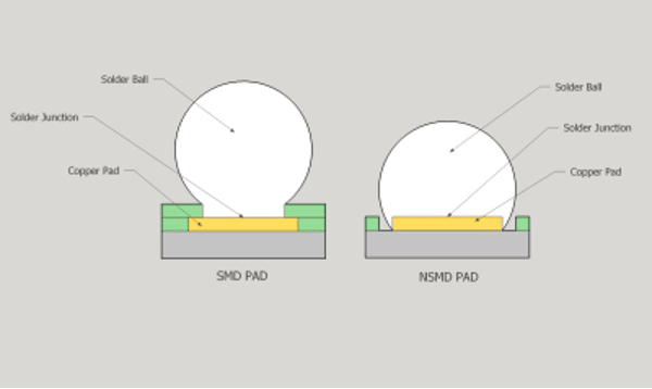
Collapsing vs. Non-Collapsing
That leads us to another aspect. Some BGA devices are designed to settle down during solder reflow. They are counting on shorter thermal paths and lower inductance. We get there with a pad that is a little smaller than the ball itself. It is by definition, Non-Solder Mask Defined (NSMD). The process allows for the ball to "collapse" over the edges of the land. There is still some air-space between the device and the board for underfill if required.
When there's no more room for that technology, we switch over to non-collapsing geometry. The balls themselves become so small that we need to keep them standing tall for the stress relief over temperature. Most sources I have found say that this switch happens at 0.5 mm while I just wrote that It is mandatory at 0.35 mm pitch. I know what I have read, and I know what I have actually done. If you find yourself somewhere in the grey area, consult the data sheet and run it past your favorite fab house.
Hey, thank you for your time spent reading my little story on BGAs. As alternates become harder to find and HDI boards become the norm, it is inevitable that you will eventually run into the same problems I have been solving. I hope this helps.
Want some more? Here are some deeper dives from folks who know what they are talking about:
- TI BGA reference guide – It is not unusual for me to reference documentation from Texas Instruments and this is no exception. This is the stuff we knew 18 years ago, but it is a good start.
- Intel BGA Databook – Whenever you want too much information, just ask Intel.
- The Coefficient of Thermal Expansion – If I did not get into enough detail about the physics, this outfit has you covered. it and deserves credit for the first diagram
- Finally, Siddarth Bind pulled these diagrams together with a crisp explanation of the two methods for defining the BGA footprint.