Sharing IP Blocks Across Different Designs - How Reuse Saved My Carpal Tunnel (Career!)
Design reuse comes in several flavors. One of the most common is applying the same electronics to different form factors. The most interesting examples come from my start-up days. The first serious reuse I got to do was based on optical transponder technology in the highly competitive OC192 - 10 GB/s market.
Like other areas in enterprise hardware, the form factors are based on Multiple Source Agreements. Companies in a particular arena agree to use the same connectors and other parameters set forth in the MSAs. Those agreements are referred to as de facto standards. Every so often, the vendors got together for a “Plug Fest” to measure interoperability.
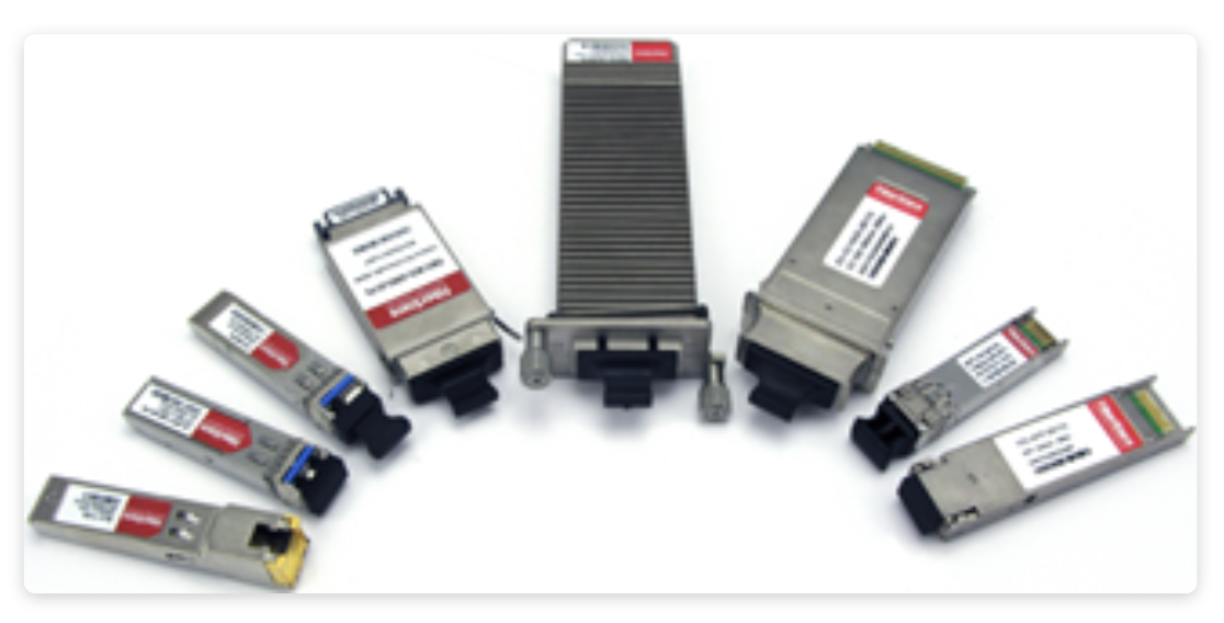
Image Credit: Cable Solutions - One function, many flavors
As you can see, there isn’t always an agreement so a proliferation of form factors results. From a candy bar to a pack of gum, the products fit into several buckets including XAUI, ZENPAK, X-PAK, X2, and SFP+. Taking the three largest ones in the middle, you get long and slender to shorter and wider and something in between. In order to effectively reuse the PCB, the circuit has to be narrow enough for the long one and short enough for the wider ones.
Overlay the three PCBs that would fill the space and the electronics have to fit within the narrow and the short form factors. Selling into any single MSA would allow using all of the available board space. Supporting those three sizes constraints the design to only the common ground between them. There is a lot going on under the hood of any of these devices. The laser and the photodetector are big components that want a lot of power.
Design Reuse When Space Is at a Premium
Given the requirements and using the standard rules for temperature rise, the power plane should be approximately twice the width of the entire device. How do we do it? Use two layers! The laser and the PD take up most of the real estate on the board. How do we get the control electronics and everything else on there? Use two boards with a stacking connector. The connector itself uses about a quarter of the board space. Now what? Use both sides of both boards.

Image Credit: Author - The Daughtercard on an A/B flip panel that reuses one paste stencil no matter which side is up.
The total headroom of the MSA is not much, so the gap between the boards is only one millimeter. In order to populate the bottom side of the top board, we have to consider that the maximum component height will be constrained by whatever is placed on the top of the bottom board. Remember, the stacking connector has one millimeter of Z-height to share among the two.
Here’s how I solved that. The placement boundary shape can be given a maximum height attribute. In addition to setting the value as a property, add the maximum component height as text on that same layer. Import that image from the bottom board to the upper board. Now you have a dynamic headroom map. An inductor that is nearly one mm on one board means zero left for the other board.
“The daughtercard was one of the toughest four-layer, through-hole boards I can remember…”
In the end, there wasn’t much air-space between the boards; almost like stacking up Legos. A heat map for the placements was helpful in keeping hot spots scattered rather than concentrated. Having the Z-height attributes embedded in the footprints allowed us to check for interferences using the MCAD software. The daughtercard was one of the toughest four-layer, through-hole boards I can remember for those reasons. It fit in the socket no matter which form factor was in play.
Designing the lower board in such confined quarters would take maybe two weeks for the first iteration and less than half of a day to generate the other sizes. The edge connector moved along with the new outline and that was about it. We covered our bases that way and could satisfy Cisco first and the smaller outfits right afterwards.
Analog Design Reuse - Maximizing Sales Channels With Minimum Effort
I had a mentor in my early days who recruited me to a WIMAX company and then, after the optical stopover, to a WIFI shop where we had the rate and range to dominate the top of the market. While only 5% of the routers used our devices, they made up 20% of the market by revenue. Typical routers sold for about $50 while “Airgo inside” was good for $200. A design win with one provider meant that the others would soon follow suit. Bragging rights are important to Belkin, Linksys, Netgear and so on.
Airgo was a marketing driven company that the street would call energetic. Energetic means taping out a board on Friday and two more on Sunday. Afterall, Sunday is Monday in some parts of the world. This was just before WIFI became standard equipment in laptops or phones. An external WIFI dongle was distributed by the various service providers.
It was another case of different standards for the same thing. You had your PCIe, MiniCard, Half-MiniCard and USB dongles for the 802.11.N spec. Airgo’s OFDM technology was adopted for N-routers; astonishing for a little start-up to win in such a competitive market.
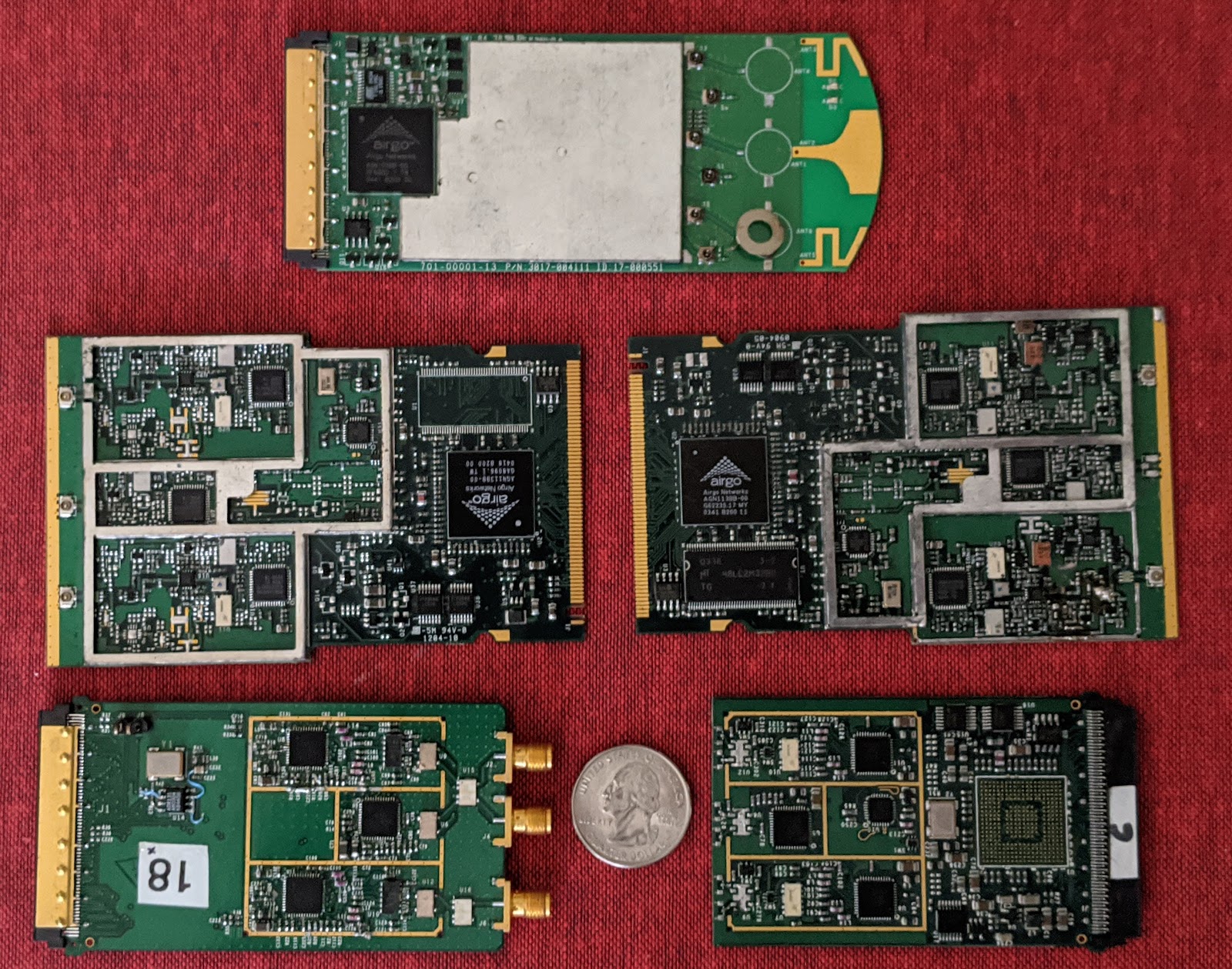
Image Credit: Author - Various WIFI Dongles
The CEO had two metrics that mattered. “When can I have customer samples?” and “When can I have 10,000 units on a boat? The Marketing team, a group of well-dressed Italian “paisanos” weren’t going to tolerate much time between the two milestones. Getting the SKUs all done in a hurry wasn’t an offer that could be refused, if you know what I mean.
RF is a tricky and sometimes unpredictable science. A batch of first-born PCBs came from the factory with a spurious emission. We couldn’t get the other form-factors out the door until the spur was brought under control. The answer was adding a big stub of copper right where the EE wanted it.
“leveraged a script of the process that was redundant for the other boards”
Of course, the tuning stub had to go where a number of components were happily placed. The parts that were in the way were removed from the virtual board and were handled like new components. I leveraged a script of the process that was redundant for the other boards and new revisions were taped out all on the same day.
Design Reuse for Advanced Technology Applications
More recently, I used a similar process to revise a set of eight PCBs that used the same logic but with slightly different board outlines. Each of the eight boards carried 16 channels. Replacing a part in one channel meant that 127 others also had to be upgraded. The only way I could get that done was with reuse modules that could be redefined and globally updated.

Image Credit: Dave Hall, CEO of Velodyne Lidar - If he can show it to the world, then so can I
Scripts were also in play for any work unrelated to the individual channels where there were only seven copies. Capturing a script for the first one and running it on the second one saved a lot of time. If anything was overlooked, then capture the fix and run that script after the first script when it came to the third board. Doing eight tape-outs over the course of one day became routine after a while. Thinking ahead to avoid repetition gives a Designer more time to do it right the first time. Try it. Your carpal tunnels with thank you.