Common Design For Assembly "Gotchas"
Adding Value to the Tail End of the Production Line
Great ideas come together with great timing and the only thing left is great execution. Flipping the switch that sets the factory in motion will cause a few pain points. These “opportunities for improvement” will dictate your agenda down to the minute with all the little things that go wrong. Let’s say that there is a factory right downstairs from you. Further, the factory is doing slow and laborious rework on old Printed Circuit Boards, AKA PCBs. There is a solution! New PCBs; we’re going from P0 (zero). To P1 (one). That’s where we, the Designers, come in.
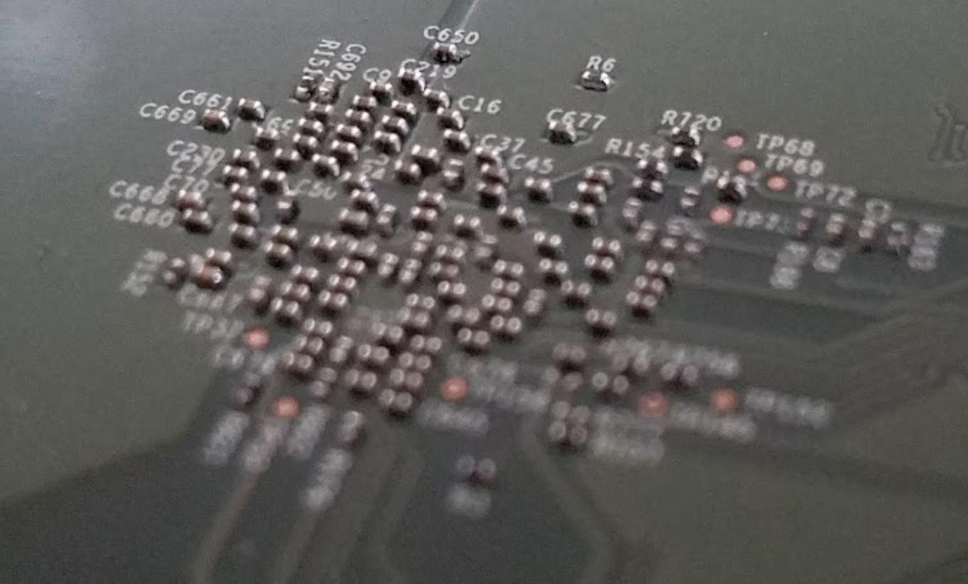
Image credit: Author: a cap-hungry MCU lives on the other side
The first order of business when it is new-PCB time is improving the electronics in some way. The fix could be better performance, lower cost, higher reliability and in some cases, all of the above. Venturing into the wireless technology and gaining FCC approval to play in their allocated spectrum is not a slam dunk. Beefing up the power grid is a typical step. A good power distribution network has been known to cover for some otherwise iffy routing. Every engineer will have some considerations carried forward.
Remember those last minute patches to fool the Design Rule Check (DRC) into giving a pass to the intentional short from one one ground domain to another? No? Now would be an appropriate time to address that sort of thing. Test access anyone? More hooks to keep tabs on the current density are always a welcome addition.
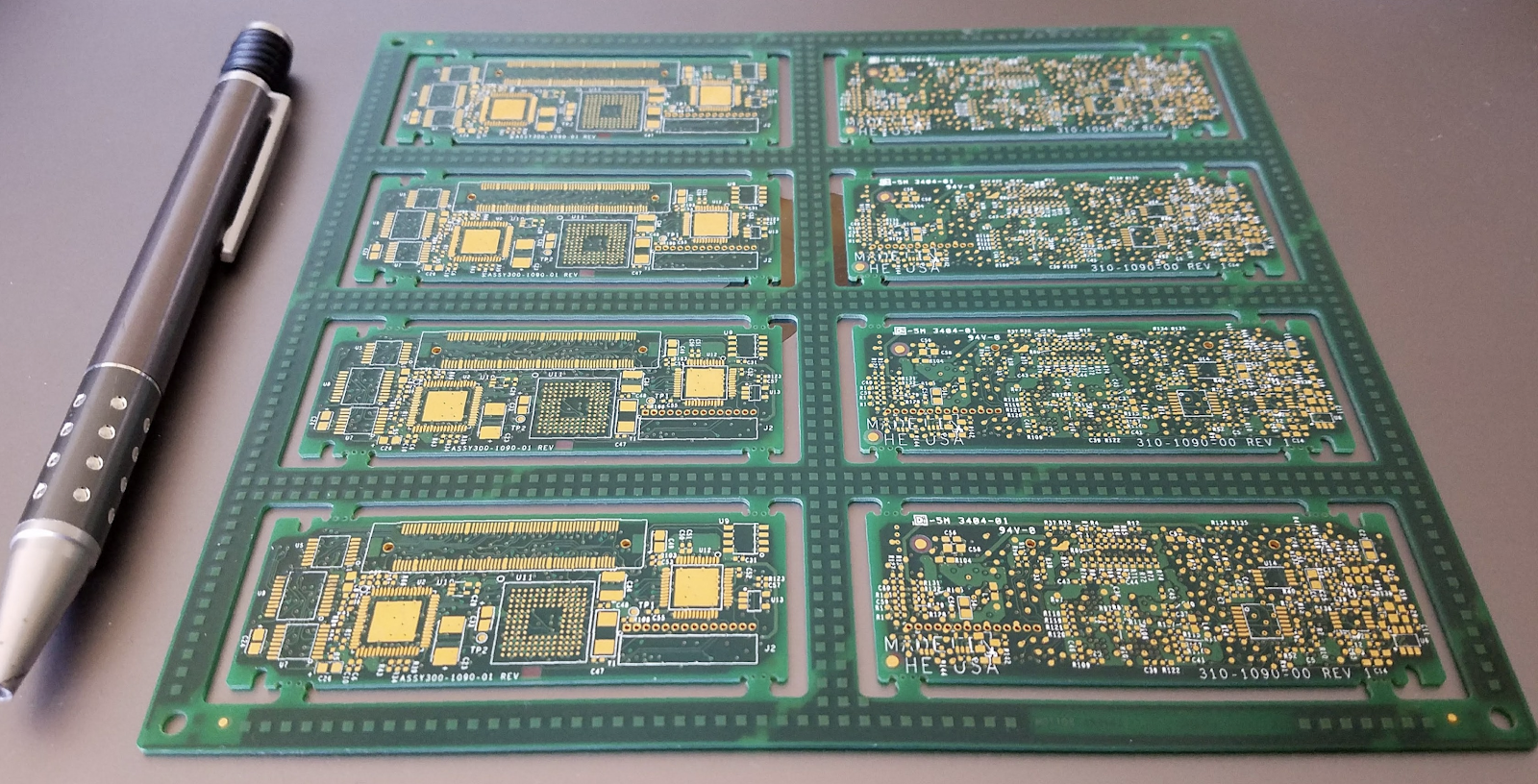
Second order of business is getting the fab shop to build to the print. The P1 version is when the final form factor is in play. That only matters to the extent that it sets the size limit. For your information, the limit shrinks constantly. Having collected data from the P0 build, there is some confidence in the all-important stack-up data along with impedance calculations. Capturing all of that for posterity is a big deal.
A perspective I like to give is that I think of DFM as Design For Money. Manufacturing is where the money changes hands. The product goes in one direction and money flows back towards the source of the goods. If you’re any kind of capitalist, you want to keep that machine running. Do not turn it off or even slow it down.
Some Assembly Required
Finally, handing a set of clear plans to the assembly house is way more important than building a flat-pack shelving unit. Numbers of holes on the drill chart need updating. XY machine data. Critical dimensions and other mechanical relationships are added for clarity. Anything that bubbles up out of the original design gets squared up on the second revision. In some cases, retrofitting new data can take more effort than the original creation.
The Simple Things
Some smart alec once said that a man with two watches never knows what time it is. Producing data in two popular formats is tantamount to giving your vendor an extra watch. Once and only once. That is to say that all of our data has to be congruent in terms of part numbers and revisions and properly put to bed. One complete set of information without overlap/repetition of the data.
An assembly drawing is just that. The soldering profile, stencil thickness, paste composition and so on are relevant but they ought to belong to a process document. This advice is more about passing ISO audits than helping your assembly line worker do their job with a one-pager on a particular PCB Assembly. Separate “what is” from “how to”.
If you choose the other path, remember to circle back to your assembly line to see if any alterations were made to your stencil artwork. There are a number of global micro-edits at their disposal when it comes to dialing in a stencil. I try to avoid getting the assembly drawing involved with the churn of process methodology on the assembly floor.
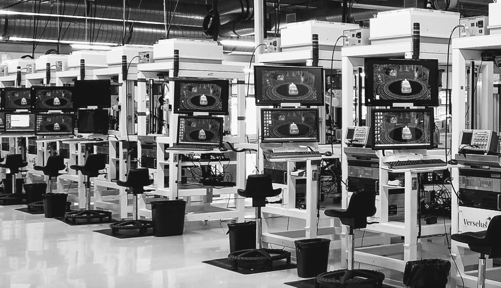
Image credit: Author - Semi-automated assembly
If there’s a conflict between the information on the PCB silkscreen marking vs. the information on the assembly drawing, it can disturb the people involved with making those products. Your only defense against this type of transgression is to spend a little time pouring over the details of file names and such to make sure that nothing is ambiguous.
I don’t know who said it but a little gem someone gave me is this: “If something can be misunderstood, then it already has been.” The automotive industry borrows a word from the Japanese, poka-yoke (ポカヨケ). The essence of this concept is that something will fit together if and only if it is being assembled correctly. It could be the reason that three tooling holes are preferred to four on the assembly subpanel. In English slang, Idiot Proofing would work as a harsh translation.
So, first electrical debug and then, mechanical fit, and finally, placement, as it relates to assembly concerns, are solved. I think the reason for this hierarchy is the immediacy of the team members. PCB Designers are inevitably linked to the Electrical Engineers first even (or especially!) when their original background was mechanical engineering. Our world is a blend of those three things that are occasionally (read always) at odds with one another.
Because the assembly takes place at some distance in both space and time, it is easier for them to fall off of the radar. The board designer is their champion from the smallest component placement decision on up to the final design review. We’re at our best when we can integrate all of these things so that the line keeps on moving and moving.