Creating and Managing a PCB Layout Database for Success
Key Takeaways
-
Verified component libraries and reuse of trusted reference circuits help prevent design errors and delays.
-
Embedding design rules, managing constraints, and using version control are essential for maintaining database integrity.
-
OrCAD X enhances PCB database management with dynamic BOM updates, constraint management, cloud libraries, and collaboration tools.

Managing a PCB layout database is key to a reliable PCB production workflow.
For beginners and seasoned engineers designing printed circuit boards, understanding a PCB layout database is key to building reliable, manufacturable boards. Let’s dive into what PCB layout databases are and explore their practical and technical applications.
A PCB layout database is the complete, organized repository of all the information needed to design, verify, and manufacture a printed circuit board. It holds everything about your design:
-
Component footprints
-
Netlists (electrical connectivity)
-
Design rules
-
PCB layers
-
Trace layouts
-
3D mechanical data
-
Simulation models
-
Manufacturing outputs (Gerber files, ODB++, IPC-2581)
Without a well-structured PCB layout database, your design can quickly spiral into chaos, leading to delays, manufacturing errors, or complete project failure. Your PCB layout database is your single source of truth — your design, your knowledge, your intent — all bundled into a structured form that your design tools and manufacturing partners can understand.
Key Elements in Organizing a PCB Layout Database
Component Libraries: Verified and Trusted
One huge insight from the engineering community is the importance of reliable, verified component libraries. People often mistakenly assume you can just download random parts off the internet. Big mistake! Instead:
-
Use trusted libraries from major vendors (like Digi-Key’s libraries, Ultra Librarian, or Octopart).
-
Pull component symbols and footprints directly from IC vendors’ reference designs.
-
Explore tools like Ultra Librarian, which gives you 16 million+ verified parts across your EDA platforms.
|
Pro Tip: Always check footprints against the datasheet! Even "verified" libraries can occasionally have minor mistakes. |
Reference Circuits and Reuse
You won't find a "perfect drag-and-drop" circuit for every HDMI port, SD card reader, or USB-C interface you want to build. The most reliable circuits are:
-
Hidden inside datasheets or application notes
-
Bundled with evaluation boards or reference designs
Instead of wasting time reinventing the wheel, reuse proven circuits wherever possible — but continually adapt them to your project’s needs!
Rules, Constraints, and Verification
Good PCB layout databases embed design rules directly inside the project. These rules govern:
-
Minimum trace widths
-
Clearance between traces
-
Differential pair matching
-
Impedance control
-
Power integrity constraints
Many modern tools automatically check DRC (Design Rule Checks) and ERC (Electrical Rule Checks) as you work. Use them religiously!
|
Pro Tip: If you’re planning high-speed or RF boards, using tools like OrCAD X is highly recommended due to their integrated SI/PI (Signal Integrity/Power Integrity) analysis. |
Managing Your BOM and Manufacturing Files
A full PCB layout database should also tie into your BOM management:
-
Include part numbers, suppliers, pricing, and availability
-
Track alternatives in case of shortages
-
Connect the mechanical 3D models for final product visualization
Best Practices for PCB Layout Database Management
Here’s a checklist for success:
-
Maintain a centralized component library
-
Validate every component against the datasheet
-
Reuse trusted reference circuits when possible
-
Embed rules and constraints directly in your database
-
Keep good version control
-
Validate outputs with DFM/DRC/Verification tools
-
Always backup your database!
Your PCB layout database isn’t just "where the design files live" — it’s your entire design ecosystem. It’s your bridge between your idea and a real, manufacturable product. By staying organized, using trusted resources, and building a robust database, you save yourself a ton of rework, missed deadlines, and even reputation risk. Whether you’re a student engineer, hobbyist, or working on cutting-edge high-speed systems, how you organize your PCB layout database determines your success.
How OrCAD X Enables PCB Layout Database Management
OrCAD X provides several features that support the organization and maintenance of PCB layout databases, here are some to highlight:-
-
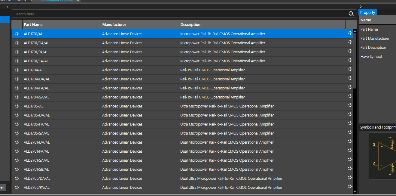
Component Information System (CIS): This system integrates a component database into the CAD environment, allowing access to component parametric and supply chain information, symbols, and footprints directly in OrCAD X Capture.
-
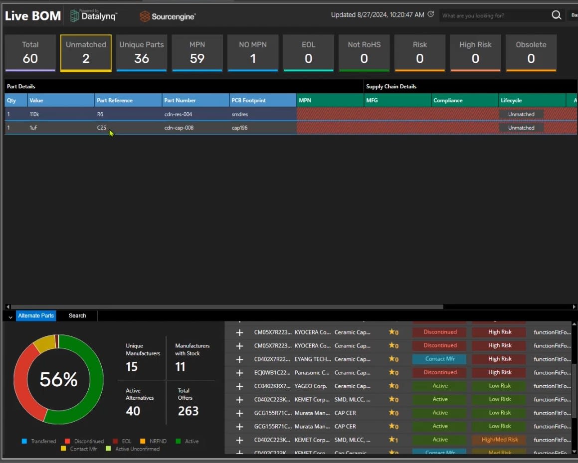
Live BOM: Provides real-time updates for over 1 billion components, enabling designers and procurement teams to stay ahead of supply chain issues.
-
Constraint Management: Manages physical and electrical constraints across schematic, PCB layout, and analysis, ensuring design accuracy and compliance.
-
Design Collaboration: Up to two users can work concurrently on the same PCB design, enhancing team collaboration and efficiency. -

OrCAD X Live BOM automatically provides real-time updates for your components.
OrCAD X Features Supporting PCB Layout Database Management
|
Feature |
Description |
How It Supports PCB Layout Database Management |
|
Component Information System (CIS) |
Integrates component databases for efficient management of components in designs. |
Centralizes part data (symbols, footprints, attributes) inside the design database. |
|
Live BOM |
Offers real-time BOM updates and supply chain insights for over 1 billion components. |
Keeps the database BOM accurate, up-to-date, and synchronized with sourcing realities. |
|
Constraint Management |
Provides a centralized system to manage design constraints across various stages. |
Embeds electrical and physical rules directly into the design database, ensuring consistency. |
|
Team Collaboration |
Enables real-time, concurrent PCB design collaboration among two users. |
Up to two engineers can update the layout/database simultaneously without conflicts. |
|
Live DOC |
Ensures that layout and documentation remain aligned during production preparation. |
Automatically syncs documentation and layout data inside the database. |
|
Cloud Workspaces |
Allows design data storage and sharing in the cloud, facilitating remote collaboration. |
Provides version-controlled, centralized access to layout databases across teams. |
|
Cloud Library Integration (Ultra Librarian, SamacSys, SnapEDA) |
Cloud providers provide direct access to millions of verified symbols, footprints, and 3D models. |
Reduces manual library creation errors; ensures consistent, validated data inside the PCB |

OrCAD X integrates seamlessly with major cloud-based component providers such as SnapMagic.
Cloud Library Integrations in OrCAD X
OrCAD X integrates seamlessly with major cloud-based component providers like Ultra Librarian, SamacSys, and SnapMagic, giving designers direct access to millions of verified symbols, footprints, and 3D models within the OrCAD X environment.
-
Ultra Librarian Integration: Search, preview, and drag-and-drop verified components directly into designs. Ensures model accuracy and reduces manual library maintenance.
-
SamacSys & SnapMagic Integration: Access large inventories of validated parts, helping streamline schematic capture and layout without leaving OrCAD X.
-
Component Information Portal (CIP) Integration: This integration automatically links cloud-sourced models to your local component database for better data consistency.
By leveraging these cloud providers, OrCAD X enables faster part sourcing, improves BOM accuracy, and ensures PCB layout databases remain consistent, complete, and manufacturing-ready, minimizing manual errors and saving time.
Organizing a PCB layout database is essential for ensuring PCB designs are manufacturable, accurate, and ready for production. Cadence's OrCAD X platform helps engineers centralize components, manage live BOMs, enforce constraints, and collaborate seamlessly across teams. Explore the full capabilities of OrCAD X and start a free trial today to optimize your PCB layout workflows.
Leading electronics providers rely on Cadence products to optimize power, space, and energy needs for a wide variety of market applications. To learn more about our innovative solutions, subscribe to our newsletter or our YouTube channel.