Rigid-Flex PCB Strain Relief Designs: Best Practices With OrCAD X
Key Takeaways
-
Strain relief at the transition points of rigid-flex PCBs is crucial for preventing damage due to bending or manipulation.
-
Key design aspects include maintaining a minimum height difference, ensuring sufficient flex section length, avoiding components in high-stress areas, and calculating the appropriate bend radius.
-
Strain relief involves applying a flexible, bead-like epoxy or silicone using precision tools at the flex-rigid junctions.
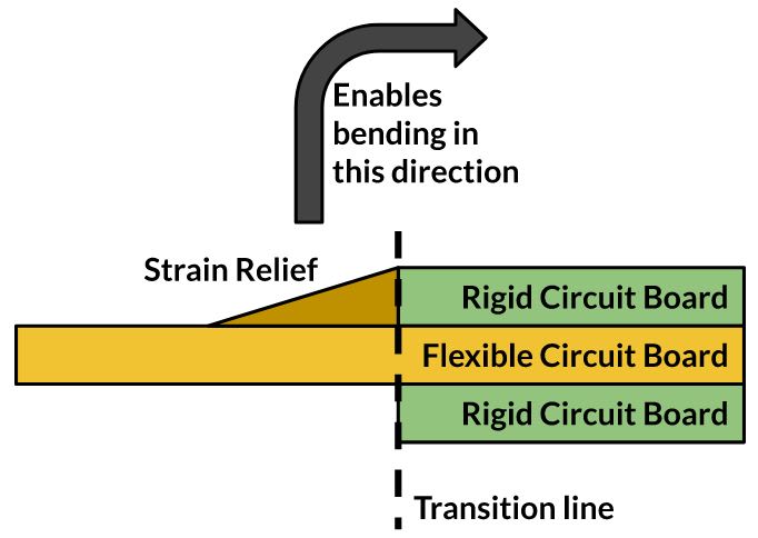
Rigid-flex PCB strain relief is shown as a tapered filet.
An important design aspect in rigid-flex PCB design is the transition line(s) between a flexible section and rigid section. To alleviate strain in rigid-flex or flex circuits, a flexible material bead is applied at the transition, known as a rigid flex PCB strain relief. Once this material sets, it forms a tapered filet (shown above).
Common Types of PCB Strain Relief
|
Type of PCB Strain Relief |
Description |
|
Stiffeners |
Rigid materials like FR4 or polyimide are attached to the flex PCB to provide additional support and prevent bending or twisting. |
|
Adhesive Tapes |
Double-sided tapes are applied to the flex PCB to offer extra support and prevent bending or twisting. |
|
Cable Ties |
Plastic or metal ties are used to secure the flex PCB to a rigid structure or component, thus preventing bending or twisting. |
About Rigid-Flex PCB Strain Relief
The primary function of rigid-flex PCB strain relief is to shield components from stress incurred during bending or manipulation at a design's transition point. Issues can arise in rigid-flex circuits or flex designs with stiffeners where the flexible circuit layers emerge from rigid areas. If a bending requirement is near the transition, it might force the flex layers to bend sharply, creating a crease that surpasses the maximum bending capacity of the flex layer's construction. Such a sharp bend can deform the copper circuits, causing them to harden and become less ductile.
Rigid-Flex PCB Strain Relief Design Considerations
|
Design Requirement |
Description |
|
Minimum Rigid to Flex Height |
|
|
Flex Section Length |
|
|
Application Sides |
|
|
Bend Area Design |
|
|
Conductor Spacing and Bend Radius |
|
|
Conductor Width |
|
|
Air Gap in Rigid-Flex |
|
|
Thermal Expansion |
|
How Rigid Flex Strain Relief Is Applied
At the junction of the flexible and rigid sections of a circuit, a small bead of polymer is applied to mitigate physical stress at the interface. This strain relief material could be a flexible epoxy, acrylic, RTV silicone, or polysulfide compound. Application is typically carried out using either a manual or pneumatically assisted syringe. The horizontal dimension of the strain relief typically ranges from 1.0mm to 2.5mm.
OrCAD X for Rigid-Flex PCB Design
|
Feature in OrCAD X |
Description |
Benefits of Rigid-Flex PCB Strain Relief |
|
Enables visualization of rigid and flex designs within tight enclosures, incorporating material flexure and bend radii adjustments. |
Allows designers to optimize the assembly of systems, reducing potential errors related to mechanical integration. Useful for ensuring that strain reliefs are positioned accurately to manage stress transitions. |
|
|
Cross Section Editor |
Provides a tool to define and visualize the cross-sectional layers of the PCB, enabling the differentiation between rigid and flex areas along with the application of various stack-ups. |
Aids precise design of transitions and stack-ups at strain relief points, ensuring proper thickness and material properties are maintained to prevent bending and twisting at critical areas. |
|
Import and Export of Mechanical Data (IDX Import) |
Allows the importation of mechanical design data, including defined zones and bends, from external mechanical tools into OrCAD X. |
Ensures the mechanical and electrical designs are aligned, which is vital for applying strain reliefs where mechanical stress is anticipated during flexing. |
|
Supports exporting 3D data of the board design in multiple formats for ECAD and MCAD analysis. |
Useful for evaluating the physical assembly and integration of the design, ensuring that strain reliefs function as intended under real-world mechanical stresses and movements. |
|
|
Interactive 3D Visualization |
Offers tools to visualize and manipulate the design in 3D, including bending flex regions and running collision detection. |
Verifies the spatial arrangement and mechanical clearance of components in flex regions, ensuring that strain reliefs are effective and do not interfere with other components. |
To experience all the features geared for rigid flex PCB strain relief design, learn more about OrCAD X here. Discover how OrCAD X can streamline your PCB design process and enhance project outcomes.