PCB Layout Planning for Footprint and Routing
Key Takeaways
-
Effective PCB layout planning improves design efficiency by structuring footprints, placement, and routing strategies.
-
Footprint management ensures alignment with design rules and manufacturing requirements for reliable assembly.
-
Cadence OrCAD X tools provide advanced features for BOM validation, footprint alignment, and real-time DRC checks.
PCB layout planning involves footprint management, in addition to layout and routing preparations.
Through PCB layout planning, engineers can take a structured approach to footprint management, component placement, and routing, saving time. PCB layout planning involves arranging components, defining connections, and preparing for manufacturing, ensuring that the design meets electrical, spacing and physical requirements before the actual layout stage.
Footprint Management in Layout Planning
Footprints are integral to layout planning, as they define the physical characteristics of components and their placement on the PCB. Key aspects of footprint management during the PCB layout planning stage include:
-
Footprint Selection: Ensuring the correct footprints are chosen for all components based on the manufacturer’s datasheets. This avoids mismatches during manufacturing and assembly.
-
Standardization: Using standardized footprints where possible to improve consistency and compatibility with automated assembly processes.
-
Spacing Requirements: Managing pad-to-pad and component-to-component spacing to prevent solder bridging and allow for effective soldering during manufacturing.
-
Thermal Considerations: Placing components with heat dissipation needs in mind and ensuring footprints account for adequate thermal vias or pads.
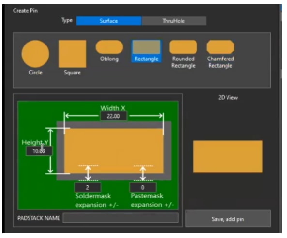
OrCAD X padstack editor allows for footprint editing.
How To Prepare Footprints for Layout
|
Category |
Guideline |
Purpose |
|
Verify Component Datasheets |
Use manufacturer-provided datasheets to ensure footprint dimensions (e.g., pad size, pitch, and outline) match the physical component specifications. |
Ensure compatibility with the physical component. |
|
Follow IPC Standards |
Adopt IPC-compliant footprint designs to ensure compatibility with industry norms, focusing on aspects like pad sizes, solder mask bridges, and keep-out zones. |
Maintain adherence to industry standards for reliable assembly. |
|
Optimize Pad Dimensions |
Define pad dimensions based on component types, ensuring adequate space for soldering without bridging or assembly issues. For exposed pads, segment them for better soldering results. |
Enhance solderability and assembly reliability. |
|
Include Orientation and Polarity Indicators |
Add markers for pin 1, component orientation, and polarity (for diodes, capacitors, etc.) on the silkscreen to prevent assembly errors. |
Prevent assembly and alignment errors. |
|
Design for Manufacturability (DFM) |
Ensure footprints provide adequate clearance from the PCB edge, other pads, and drill holes. Incorporate keep-out zones to prevent routing conflicts. |
Improve manufacturability and reduce production issues. |
|
Minimize Assembly Risks |
Use symmetric pad layouts to avoid tombstoning and maintain consistent solder fillets. Ensure pads are adequately spaced for stencil printing. |
Reduce soldering defects and improve assembly quality. |
Planning for Specialized Components
-
Surface-Mount Devices (SMDs): Focus on precise pad definitions, keep-out regions, and solder mask bridges.
-
Through-Hole Components: Define drill hole sizes, annular rings, and pad stacks for robust mechanical connections.
-
High-Pin-Count Components (e.g., BGAs): Plan for proper pitch, alignment, and thermal management, especially for high-density designs.
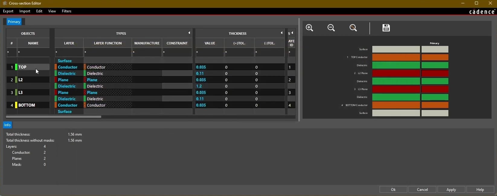
OrCAD X cross-section editor.
Other Considerations in PCB Layout Planning
After defining and verifying footprints in the PCB layout planning stage, the focus shifts to aligning components and organizing the PCB for efficient routing and manufacturability. Engineers should consider:
-
Functional Grouping: Positioning related components close together to minimize trace lengths and improve signal integrity.
-
Signal Prioritization: Planning the layout of high-speed signals, sensitive analog lines, and power distribution early in the process.
-
Mechanical Constraints: Ensuring alignment with enclosures, connectors, and mounting holes while leaving sufficient edge clearance.
-
Thermal Design: Strategically placing heat-generating and heat-sensitive components to optimize airflow and cooling.
Aligning components with these considerations in mind streamlines the design process and ensures the board functions as intended.
PCB Layout Planning Considerations
|
Preparation Stage |
Key Details |
|
BOM Validation |
- Verify manufacturer part numbers (MPN) and vendor part numbers (VPN). - Check for component availability to avoid obsolete parts or long lead times. - Mark Do Not Install (DNI) components correctly in the BOM. |
|
Stack-Up Design |
- Select materials (e.g., FR4, Rogers) based on frequency and environmental needs. - Define the number of layers for signal, power, and ground planes. - Establish controlled impedance (e.g., 50Ω single-ended, 100Ω differential). - Choose copper thickness (½ oz, 1 oz, or 2 oz). |
|
Design Rule Definition |
- Set electrical rules for impedance, resistance, and high-frequency designs. - Define physical rules for trace widths, via sizes, and clearances. - Specify spacing rules for traces, vias, and copper-to-edge distances. |
|
Schematic and Netlist Preparation |
- Create component symbols with reference designators linked to their footprints. - Ensure netlists clearly define connections and critical signal paths. - Mark impedance-controlled traces and power nets for easy identification. |
|
Board Outline Definition |
- Define board dimensions and shape manually or by importing CAD data. - Align the outline with enclosure designs and mechanical constraints. - Leave adequate edge clearance for traces and components. |
|
DFM Considerations |
- Maintain minimum trace widths and spacing per fabrication guidelines. - Avoid complex assembly features like via-in-pad unless necessary. - Ensure silkscreen and solder mask layers are legible and clear. |
How to Use OrCAD X For PCB Layout Planning
|
PCB Layout Planning Element |
OrCAD X Tools for PCB Layout Planning |
|
BOM Validation |
- Use Live BOM to synchronize design data with real-time component availability. - Validate manufacturer part numbers (MPN) and vendor part numbers (VPN). - Mark DNI components directly in the BOM editor. |
|
Stack-Up Design |
- Use the Cross-Section Editor to define and visualize PCB stack-ups, including material properties, layer count, and thickness. - Incorporate controlled impedance requirements like 50Ω single-ended and 100Ω differential pairs. - Visualize copper thickness and assign power or ground layers during stack-up definition. |
|
Design Rule Definition |
- Set electrical, physical, and spacing rules in the Constraint Manager, covering impedance, trace widths, and via sizes. - Define advanced constraints, including differential pairs, HDI designs, and via stacking. - Use the DRC Validation Tool for real-time checks to identify and correct violations. - Apply DFM Wizard rules to ensure compliance with IPC standards for fabrication, assembly, and testing. |
|
Footprint Management |
- Use the OrCAD X Footprint Editor’s wizard to create or verify footprints based on datasheets and IPC-compliant guidelines. - Manage pad-to-pad and component-to-component spacing to prevent solder bridging. - Validate footprint alignment using the integrated 3D Viewer Tool. - Leverage DFA Rules for spacing between components to avoid assembly issues. - Incorporate pin 1 and polarity indicators to prevent orientation errors during assembly. |
|
Board Outline Definition |
- Define the board outline in the Mechanical Layer Editor or import mechanical constraints via DXF/DWG files. |
|
DFM Considerations |
- Perform detailed DFM checks using the OrCAD X DFM Checker to identify manufacturing issues such as insufficient clearances, via-in-pad placement, or solder mask openings. - Use the Padstack Editor to refine pad dimensions and solder mask openings, reducing the risk of solder bridging or assembly defects. - Validate silkscreen clarity and ensure proper text placement. |
Ready to start tackling PCB layout planning? Cadence’s PCB Design and Analysis Software, including OrCAD X, simplifies layout planning with advanced tools for footprint management, DRC checks, and manufacturability.
Leading electronics providers rely on Cadence products to optimize power, space, and energy needs for a wide variety of market applications. To learn more about our innovative solutions, talk to our team of experts or subscribe to our YouTube channel.