How to Create a Variable Power Supply PCB Layout
Key Takeaways
-
Understand the purpose of each component in a variable power supply, including transformers, rectifiers, capacitors, and regulators.
-
Learn about different topologies for variable power supplies, from discrete resistor selection to continuously variable potentiometer-based designs.
-
Discover how OrCAD X tools like DFM, interactive routing, constraint management, and thermal analysis can streamline the design and optimization of variable power supplies.
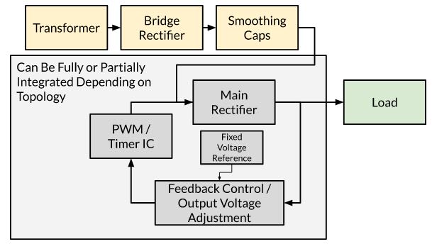
Variable power supply block diagram
A variable power supply allows the user to vary and adjust the desired output voltage and current. This type of power supply circuit includes an adjustable voltage regulator that can be set according to a specified input. An adjustable voltage regulator features both line regulation and load regulation.
Unlike fixed power supplies that provide a constant output voltage, variable power supplies can be adjusted to different output voltages as needed. In contrast, fixed voltage power supplies or battery chargers provide a single, unchanging output voltage and are designed for specific, consistent power requirements. Read on as we discuss variable power supply PCB layout tips.
Major Circuit Blocks for a Variable Power Supply in PCB Layouts
|
Component or Circuit Element |
Purpose |
|
Transformer |
Steps down the AC mains voltage to 12V AC. |
|
Full Wave Rectifier |
Converts AC voltage from the transformer to DC voltage with ripple. |
|
Capacitors |
Filter out ripples from the rectified DC voltage to produce a smooth DC output. |
|
Main Variable Positive Voltage Regulator |
Provides an adjustable positive output voltage. Depending on topology can include (or exclude)
|
|
Pulse with modulation (PWM) / Timer IC |
Operates as an astable multivibrator to generate clock pulses for switching speed (can be independent of regulator IC or part of it) |
|
Fixed Voltage Regulator / Reference |
It is used to supply a reference voltage. Some designs use a negative voltage regulator at -12V, for example, while others may use a positive version. |
|
Feedback Control Mechanism (e.g.) CMOS Decade Counter) |
Activates outputs to control voltage levels. Can also be as simple as a potentiometer. |
Creating a Variable Power Supply
There are a couple of different topologies that can be used to achieve a variable power supply. One example involves selecting between preconfigured resistor values to change the gain of the feedback loop. In this setup, the output voltage is compared with a reference voltage. By selecting the desired resistor combination, the gain of the feedback loop can be altered, resulting in discrete variable power supply outputs.
Another topology allows for a continuously variable output voltage. This is achieved using a potentiometer that modifies the feedback gain factor in the loop. By adjusting the potentiometer, the feedback gain changes, which in turn adjusts the output voltage continuously over a range.
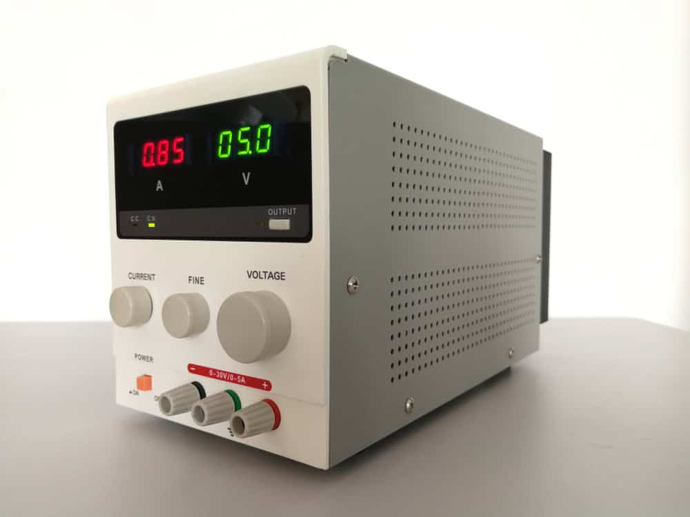
A power supply with variable output voltage.
Variable Power Supply PCB Layout Tips
Depending on your chosen topology, your layout will vary. However, below we've summarized the key components of the design, along with individual layout tips for each component.
Transformer
Place the transformer near the edge of the PCB to minimize noise coupling to sensitive areas, and ensure sufficient spacing between the transformer and other circuitry to reduce electromagnetic interference (EMI). Furthermore, use wide traces for the primary and secondary windings to handle high current and minimize voltage drop.
Full Wave Rectifier
Arrange diodes close to the transformer secondary windings to minimize trace length and reduce inductive noise. Ensure adequate thermal dissipation for diodes by using thermal vias and large copper areas if needed. Finally, connect the rectifier's ground return path directly to the main ground plane to minimize ground loops and noise.
Main Regulating Component
This component will likely produce the most heat on the board. Ensure there is sufficient copper area or a dedicated heatsink to dissipate heat from the regulator, and center it towards the middle of the board for good dissipation.
Place the regulator close to the output filter capacitors to minimize noise and ensure stable output, and place decoupling capacitors close to the input and output pins of the regulator to filter high-frequency noise.
Timer IC and Feedback Control
Route the PWM output trace away from noisy power and ground traces to maintain signal integrity. Generally, the signal paths will not be carrying much current, but it is best to keep them short. Place these components close enough to the main regulator component to minimize signal loss, but in a location where they will be less susceptible to variations in quality due to heating.
Working With OrCAD X for Variable Power Supply Layout
|
OrCAD X Feature |
How It Helps With PCB Layout |
|
DFM (Design for Manufacturability) |
Ensures the layout meets manufacturing requirements by checking for common issues, such as via-in-pad, incorrect annular rings, and other manufacturability constraints. OrCAD X provides a comprehensive set of DFM rules that help designers optimize their layouts for manufacturing. |
|
Interactive Routing |
Facilitates efficient and accurate routing of signals. The tool provides real-time feedback and visualization, helping to avoid common routing issues such as trace crossing, excessive trace lengths, and sharp angles. |
|
Constraint Management |
Enables the setup and enforcement of design constraints for trace width, spacing, and other critical parameters. This ensures that the layout adheres to electrical and manufacturing specifications. |
|
Thermal Analysis Tools |
Helps visualize heat distribution and manage thermal dissipation. This is crucial for maintaining the reliability and performance of heat-sensitive components, such as voltage regulators. |
|
Design Rule Checks (DRC) |
Automatically checks the PCB layout against predefined design rules to identify violations. This helps in catching potential issues early in the design process. Real-time DRC feedback helps ensure the design meets all necessary standards and reduces the risk of errors during production. |
|
Power and Ground Planes |
Facilitates the creation of continuous power and ground planes, which are essential for reducing electromagnetic interference (EMI) and ensuring stable power delivery to all components. |
Curious to see how OrCAD X can aid in perfecting your variable power supply PCB layout? Test out each of these powerful features for free and watch your design come to life! Dive deeper into OrCAD X today and transform your layout process with ease and precision.
Leading electronics providers rely on Cadence products to optimize power, space, and energy needs for a wide variety of market applications. To learn more about our innovative solutions, talk to our team of experts or subscribe to our YouTube channel.