PCB Layout Techniques With OrCAD X
Key Takeaways
-
Before starting the PCB layout, ensure the complete schematic, including layer stackup, dimensions, and keep-out zones, are ready and verified.
-
Components should be grouped by function to avoid noise interference and effectively manage return paths. Additionally, components should be placed away from heat-dissipating areas and board-to-wire connectors should be near the edge for easy access and organization.
-
It's essential to provide complete and detailed documentation to the manufacturer, including assembly drawings, Gerber files, and board information in standardized file formats.
It is key to be organized in your PCB layout process to avoid downstream bottlenecks
Let’s face it; the fun part of a PCB design is never placing the hundreds of components. The excitement starts when you start routing the nets together. Here are eight PCB layout techniques to ensure your design’s success.
8 PCB Layout Techniques to Ensure Smooth PCB Layouts
|
1) Have Your Schematic Ready |
Make sure that your complete schematic is ready before you start the layout. |
|
2) Verify Data Before You Start the Layout |
Verify board layer stackup, board dimensions, and keep-out zones before you begin. |
|
3) Group Components By Function |
Ensure components are grouped according to their functional block in the circuit. |
|
4) Keep Components Away From Heat Dissipating Areas |
Don’t place components near the voltage regulator, power op-amp, or other heat-emitting device. |
|
5) Place Board-To-Wire Connectors Near the Edge |
Keep board-to-wire connectors near the edge of the board, especially if the wire needs to be screwed on |
|
6) Standardize the Component Placement |
Ensure pin 1 markers are all aligned in the same direction |
|
7) Make Space For Copper Traces |
Ensure sufficient gaps for copper traces to pass through, especially near components with hundreds of pins. |
|
8) Don’t Neglect the Final Manufacturing Output Files |
Make sure you send a full and complete documentation package to the manufacturer. |
PCB Layout Techniques: The Nuts and Bolts
1) Have Your Schematic Ready
It is not unusual for those doing PCB layout to gloss over the importance of preliminary steps before placing and routing components. Because of this, design checks aren’t run, parts aren’t validated, and basic drafting tasks like cleaning up text to make it more readable aren’t followed. Those missed design checks can result in bigger issues later on in the layout process. So, do yourself a favor and ensure the complete schematic is ready before you begin the layout.
2) Verify Data Before You Start the Layout
Jump-starting your PCB layout technique before having all the board data at hand usually causes more problems than it’s worth. You may find yourself in a position where you have to rip up and modify portions of your design to accommodate a change that should have been done before you started your work. Here are a few items that you should verify first:
-
Board Layer Stackup: Make sure the board layer stackup has been finalized before you start. Adding or deleting board layers can be painful, sometimes resulting in having to redo an entire layout.
-
Board Dimensions: Moving carefully placed components because your board outline needs an unforeseen new cut-out can cost you a lot of time.
-
Keep-out Zones: These zones could be for several reasons, including mechanical, thermal, height, or sensitive circuitry. If you don’t understand these requirements before you start layout, there’s a good chance you will have to make unexpected changes later.
3) Group Components by Function
Now you are ready to place components, but take care. Improper component placement can lead to a horde of issues that affect the PCB's functionality, durability, manufacturability, and serviceability.
You should ensure the components are grouped according to their functional block in the circuit. For example, power management components shouldn’t be jumbled with analog parts and high-speed digital communication should be kept on its own. The rule of thumb is to keep the noisiest signals away from the highly sensitive ones. Also, functionally separating components gives you better control of their return path.
4) Keep Components Away From Heat Dissipating Areas
In power-demanding applications, voltage regulators can heat up significantly. Chances are, you’ve included some heat-dissipating vias to increase the heat dissipation rate. However, it is still unadvisable to place other components near the regulator. The same applies when using a power op-amp or other heat-emitting device.
5) Place Board-to-Wire Connectors Near the Edge
System installers and technicians will appreciate it if you keep board-to-wire connectors near the edge of the board, especially if the wire needs to be screwed on. Not only does it look organized, but keeping connectors near the edge prevents unwanted contact with other components on the PCB.
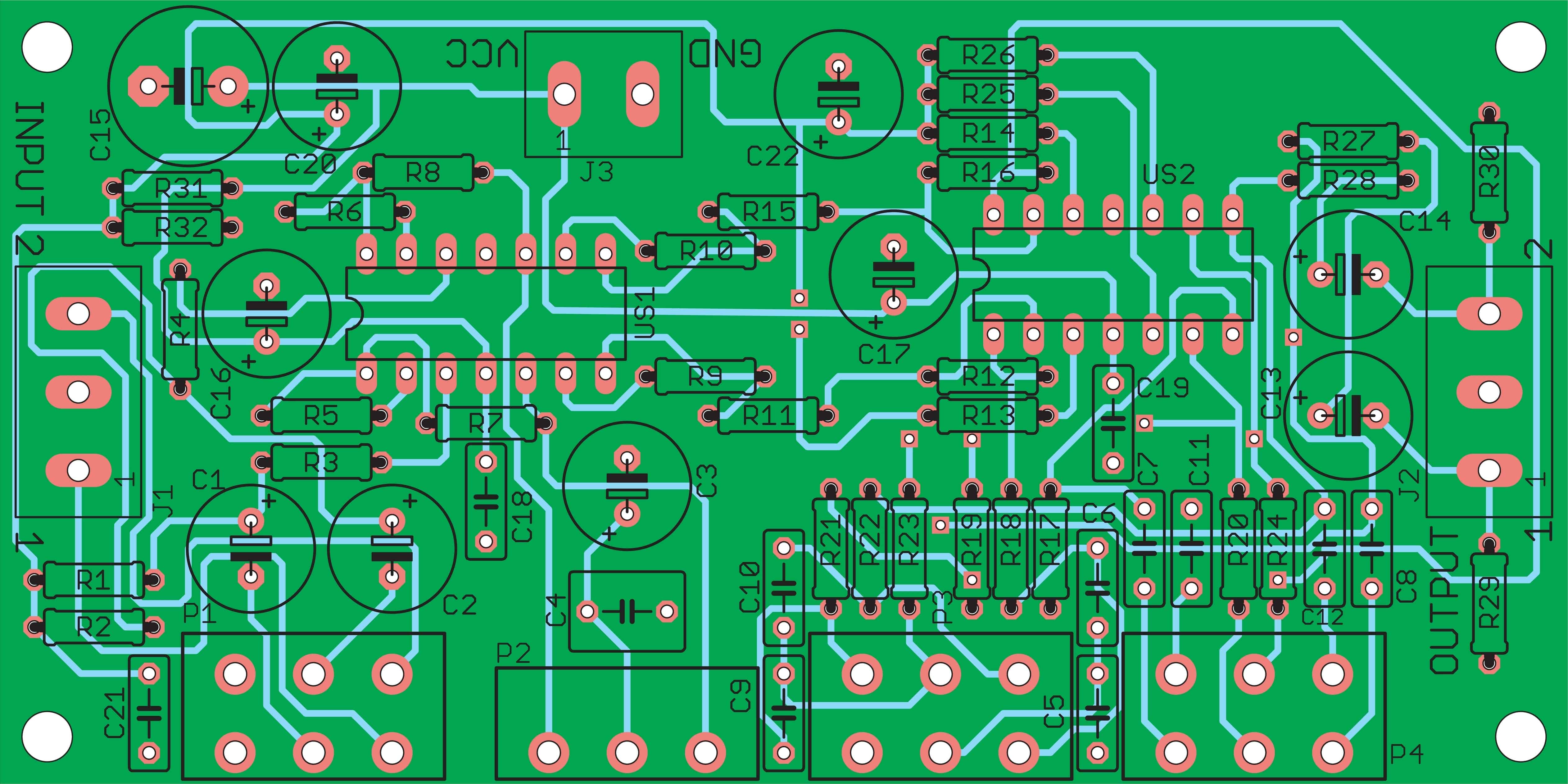
6) Standardize the Component Placement
All ICs, regardless of their footprint, have a pin 1 marker. If you don’t want your assembler to grumble each time you submit a design, ensure they are all aligned in the same direction. This increases the efficiency of the assembly process and reduces placement mistakes.
Standardized pin 1 orientation on components.
7) Make Space for Copper Traces
Modern electronics demand increasingly smaller PCBs, but sometimes there is an optimal size you need to stick with, or else you’ll find it impossible to properly route all the traces. When placing components, ensure sufficient gaps for copper traces to pass through, especially near components with high pin count. Using the Constraint Manager in OrCAD X ensures proper spacing in your design.
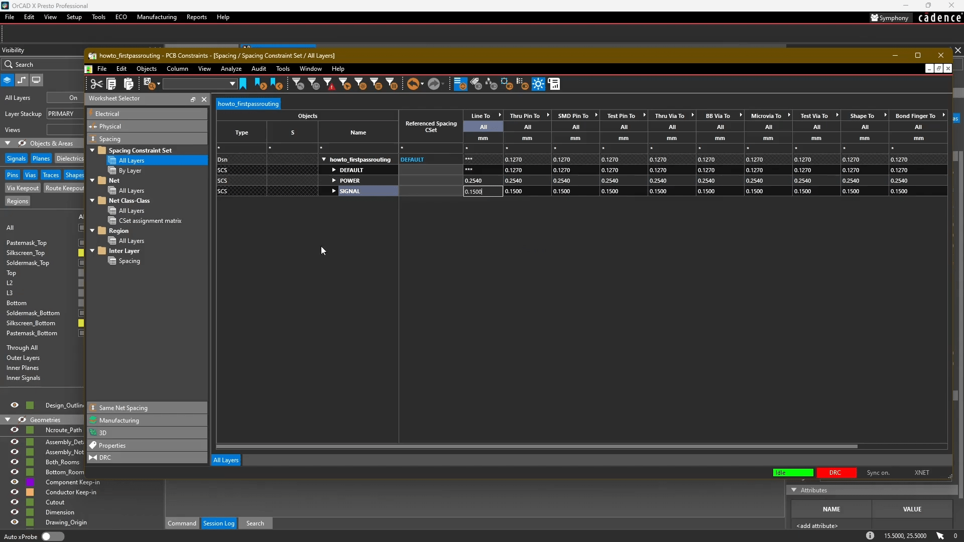
The PCB Constraint Manager in OrCAD X maintains proper spacing between traces
8) Don’t Neglect the Final Manufacturing Output Files
Managing supply chain information and component sourcing, generating assembly drawings and Gerber files, and compiling board information in standardized file formats are simple but pivotal features of the production process. The quality of your PCB is only as good as its manufacturability, so make sure to make your documentation as detailed as possible.
Communication with your PCB manufacturer or fabricator is key to reducing time-consuming bottlenecks down the line.
How OrCAD X Helps Ensure Solid PCB Layout Practices
To ensure a smooth board layout process, it's best to use advanced PCB software. Below, we've compiled OrCAD X features that aid designers in adhering to PCB layout techniques.
OrCAD X Features for PCB Layout Techniques
|
OrCAD X Feature |
Description |
|
Design Rule Checks (DRC) |
Extensive DRC capabilities ensure your schematic is complete and correct before starting the layout. |
|
Allows you to set up and finalize your board layer stackup, ensuring all layer details are correct before you begin the layout. |
|
|
Helps in verifying and setting up your physical, spacing, and other constraints before starting the layout. |
|
|
Allows you to set rules for component placement based on functional blocks, ensuring components are grouped and placed according to their function in the circuit. |
|
|
Provides 3D visualization tools to help you see how components are placed and interact with each other spatially, aiding in functional grouping. |
|
|
Supports high-density interconnect (HDI) designs, which can help manage spacing for copper traces in compact designs. |
|
|
Includes design for manufacturing (DFM) checks that help ensure the final output files (Gerbers, assembly drawings, etc.) are correct and manufacturable. |
These features in OrCAD X will help you implement PCB layout techniques effectively, ensuring a smooth design process and a high-quality final product. Learn more about how Cadence can support your design process by exploring our PCB Design and Analysis Software and OrCAD X offerings.
Leading electronics providers rely on Cadence products to optimize power, space, and energy needs for a wide variety of market applications. To learn more about our innovative solutions, talk to our team of experts or subscribe to our YouTube channel.