PCB Impedance Control With OrCAD X
Key Takeaways
-
Trace width and thickness determine the impedance and flow of current within a circuit board.
-
Controlled impedance ensures signal integrity, especially above 100MHz.
-
The PCB trace impedance increases as the width decreases.
Mismatched impedance is detrimental to high-frequency signals, especially when the frequency is above 100MHz. This can affect the integrity of both analog and digital signals. For this reason, PCB impedance control is an important design constraint when working on high-frequency circuits. By controlling the PCB impedance, unexpected damages or errors can be limited to some extent. Read on as we discuss PCB impedance control, the factors influencing it, and how OrCAD X aids in PCB impedance control.
Where does PCB Impedance Come From?
In PCBs, traces are routed to transmit signals between two points. These copper traces are sources of impedance in PCBs. Trace width and thickness play a large role in the impedance and flow of current within a trace in a circuit board. Other factors that affect trace impedance are:
-
Vias
-
The thickness of the prepreg material on the two sides of the trace
-
The dielectric constant of the core and prepreg material
-
Separation from the reference copper plane
-
The presence of solder resist
The Importance of PCB Impedance Control
It is difficult to find a trace with the same characteristic impedance throughout its length. If a signal is passed through such a trace, the signal will be the same as the original with zero loss or deterioration. Such traces or transmission lines are called uniform transmission lines or traces. However, in most cases, signals encounter reflection, attenuation, and distortion due to the variations of impedance in the traces.
Conscious efforts need to be made for PCB impedance control in order to maintain good integrity. To achieve signal integrity, the traces should be designed with uniform characteristic impedance, which leads to PCB impedance control.
PCB impedance control is the method through which reasonably uniform impedance is achieved in PCB traces by taking into account manufacturing aspects. The manufacturing parameters include the width, length, and thickness of the copper traces. Through PCB impedance control, we predetermine the impedance offered by the trace to an alternating current signal. As the frequency or the length of the trace increases, PCB impedance control becomes more critical to protect the signal from degradation. PCBs incorporated in the following products are always designed with impedance control:
-
Computers
-
Mobile phones and tablets
-
Analog and digital communication circuits (RF circuits)
-
Signal processors
-
Digital cameras
-
Motor control modules
Types of PCB Traces and PCB Impedance Control
PCBs can have different types of traces. Striplines and microstrip lines are the most common types of traces seen in high-speed and high-frequency circuits. The controlled impedance method applies to any trace that handles high-speed or high-frequency signals. The types of traces where impedance control is applied are:
-
Single-ended and differential pairs of microstrip lines
-
Single-ended and differential pairs of strip lines
-
Single-ended and differential pairs of coplanar waveguides
-
Embedded microstrip lines
How Various Factors Influence Trace Impedance in PCBs
|
Factor |
Impedance variation |
|
Trace width |
Impedance increases as width decreases. |
|
Thickness of copper |
As copper thickness increases, impedance decreases. |
|
Thickness of dielectric |
The dielectric material and impedance share a logarithmic relationship. By reducing the thickness of the dielectric, impedance can be reduced. |
|
Dielectric constant |
For controlled impedance, having a low and stable dielectric constant is preferred. |
OrCAD X enables users to inspect and set specific trace impedances.
PCB Impedance Control and Impedance Measurement with OrCAD X
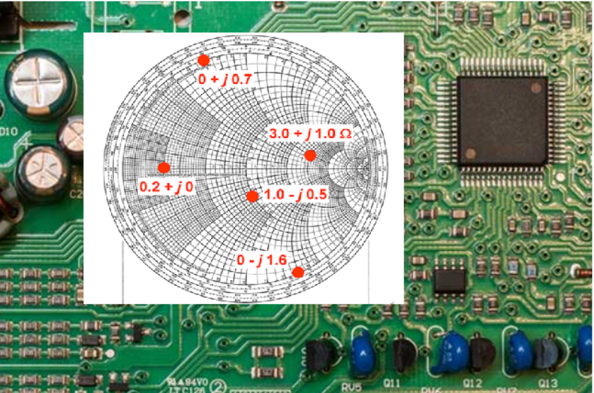
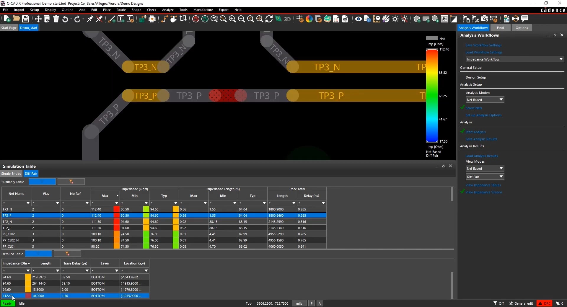
The first and foremost step in PCB design for implementing impedance control is to measure the trace impedance and make the necessary modifications to achieve the desired value. The measurement of impedance has surpassed the traditional Smith chart method, and you can use simulation tools to calculate the value. Cadence’s OrCAD X software offers powerful tools to quickly model and analyze systems effectively and provides designers with the impedance values of each trace or interconnect.
|
OrCAD X Feature |
Functionality |
Contribution to PCB Impedance Control |
|
Allows designers to perform real-time impedance analysis during PCB layout. |
Identifies traces with impedance mismatches, enabling adjustments to maintain signal integrity. |
|
|
Provides real-time analysis of coupling between traces to detect potential crosstalk issues. |
Helps in identifying and mitigating crosstalk by analyzing coupling coefficients between nets. |
|
|
Constraint Manager |
Enables setting and managing electrical constraints, including impedance and timing requirements, during the design process. |
Ensures that routing adheres to predefined impedance specifications, maintaining consistent signal performance. |
|
Provides in-design workflows for signal integrity analysis, such as impedance and coupling analysis. |
Allows designers to perform real-time impedance and coupling analysis, ensuring signal integrity is maintained throughout the design process. |
PCB impedance control is essential for high-speed circuit designs. OrCAD X allows you to analyze, simulate, and set impedance values during the design process, ensuring reliable performance from prototype to production. Try the OrCAD X Free Trial or explore the full OrCAD X platform to see how it supports precise impedance control and overall PCB design efficiency.
Leading electronics providers rely on Cadence products to optimize power, space, and energy needs for a wide variety of market applications. To learn more about our innovative solutions, subscribe to our newsletter or our YouTube channel.