Layout Strategies When Using a PCB Autorouter
Key Takeaways
-
Preparing the design for PCB autorouting
-
Effective use of a PCB autorouter
-
Different variations and capabilities of PCB autorouting
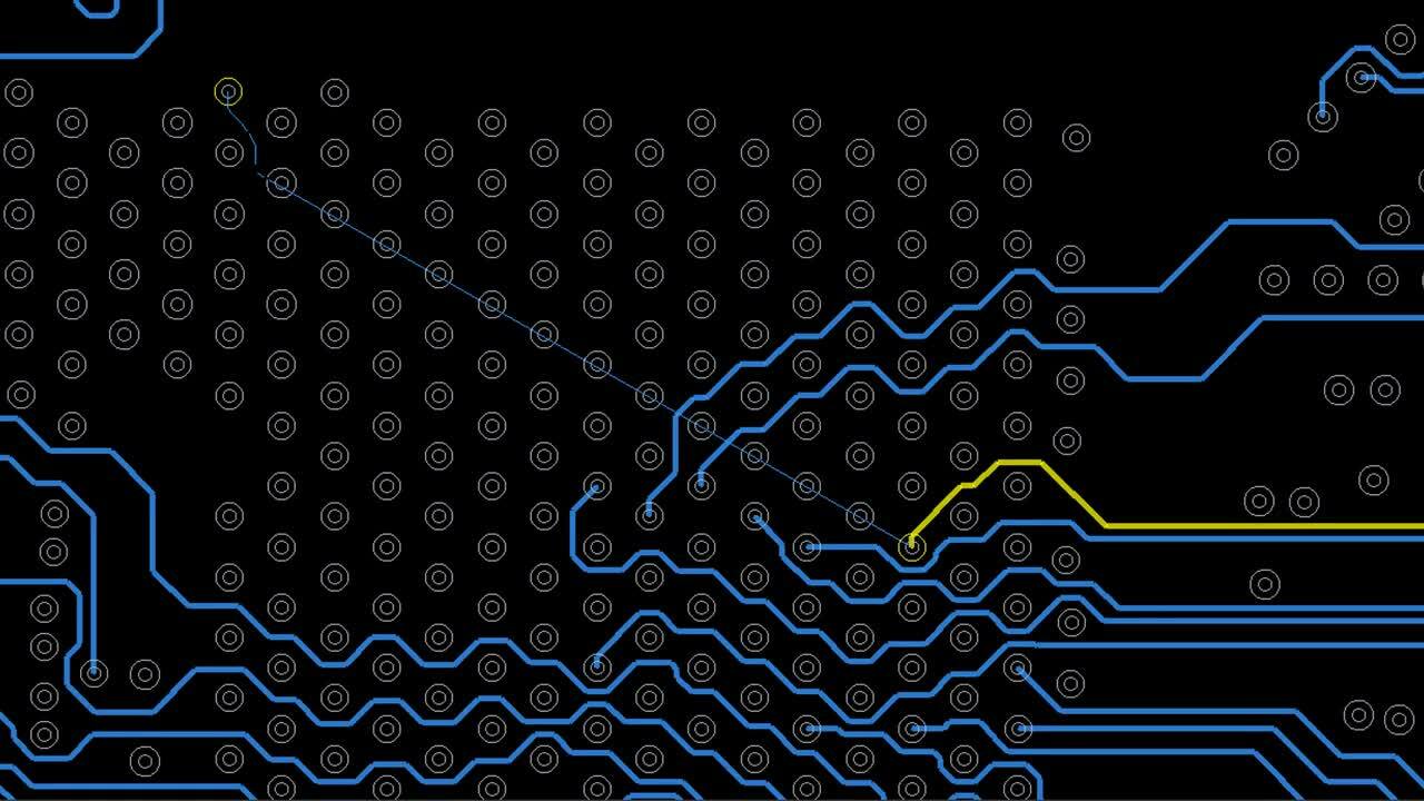
Scribble routing allows a designer to sketch the desired path of the net while the router does all the work
One of the most enjoyable aspects of PCB layout is routing the traces. Drawing lines that transform net guides into metal connections can be very cathartic, and bring with it a huge sense of accomplishment. On the other hand, manual trace routing can be very challenging, especially on a very large and intricate circuit board. It can also take a lot of time, impact design schedules, and consume employee resources. Automated PCB routing was introduced long ago to overcome these difficulties, and its capabilities have continued to grow and adapt as circuit board technologies have become more complex.
PCB autorouters were initially available only as third-party applications that were difficult to learn and use, and came with a steep price tag. Early autorouters required complex configurations and designers had to go through elaborate steps to exchange design data between the routers and their CAD systems. Additionally, the results of the early autorouters were often unpredictable, and designers were forced to spend extra time checking and polishing the routing before they could finish their designs.
Thankfully, PCB autorouting is a very different process today. Most autorouters are now built into the CAD systems that designers use to lay out their boards. These built-in autorouters have many advantages, including ease of use and superior results that make using them a useful part of the designer's toolbox. Here are some details on how to effectively use PCB autorouters during circuit board layout as well as the benefits these tools bring to designers.
Preparing Your Design for Autorouting
One of the big advantages of today’s autorouters is that many of them are built into the PCB CAD tools instead of operating as stand-alone systems. This means that the autorouters will use the same setups as the design, saving the designer from having to go through the setup process twice in two different systems. However, it is still incumbent on the designer to fully set up the design to get the maximum benefit from the autorouter. Here are some of the setups that designers need to focus on.
Design Rules
The autorouter will pull its trace widths and spacings from the existing design rules and constraints. It isn’t enough to simply set a default trace width and spacing, as the autorouter will faithfully use these values for all traces it attempts to route. Designers must go through the rules and constraints and set up net classes with the appropriate trace width and spacing set up for each one.
Routing Zones and Areas
Older stand-alone autorouting systems often required the design to be set up with specific keepout zones or blocked areas to prevent the autorouter from routing through certain areas. Once the design was pulled back into the PCB layout system, these areas would have to be removed to permit normal trace routing and editing to be done by hand. In today’s CAD systems, you simply need to configure the design with the same keepout zones as you would use for regular component placement and trace routing.
Router Commands and Configurations
Many of the older autorouting systems required multiple menus and command lines to be configured in addition to the commands and configurations required in the PCB CAD tools. Some routers required extensive scripts to be included, which designers would save and re-edit with each new design. Today’s PCB layout systems use the same types of pulldown menus as for all the other aspects of PCB design, reducing the number of different command systems the designer has to work through.
With the autorouter set up and ready to go, it's time to start using it, which we will look at in more detail next.
Two-layer routing on a printed circuit board
Using a PCB Autorouter
Using the PCB autorouter within the PCB design tools is a straightforward operation. Designers no longer have to prep and configure the design, then export it out for use by the autorouter. Instead, they will simply access a different set of menus and commands within their layout design system. In the picture below, you can see an example of the type of command menus that are available within an embedded PCB autorouter. It is important to note that many of these commands can be configured with great detail, or the designer can choose to run the autorouter in its default configuration. Simply set the system up, choose the routing option you want to use, and start the router.
Today’s autorouters have evolved quite a bit from their stand-alone forefathers and have many different options for a designer to choose from. Here are some examples:
- Escape routing: This option will only route a trace out from the surface mount pins to a via for routing on a different layer. Automated escape routing can make the designer’s job a lot easier by performing this operation very quickly.
- Trace routing: There are many ways that an autorouter can be used for routing regular traces. You can set it up to route individual nets, or batch route the entire circuit board with multiple variations between these two extremes.
- Routing cleanup: This option will remove some undesirable autorouting results like stubbed traces or loops.
Once the autorouting is done, the designer should check the results and decide whether or not to keep that iteration of routing. At this point, most designers will step in to conduct their own review and manual clean-up of the routing. If the trace routing is deemed successful, the autorouter can then be used for shielding or testpoint generation if desired.
That gives a fairly basic look at how to work with an autorouter. However, there are even more variations of autorouting technology available to designers if they choose to use them, and we’ll look more into this next.
Autorouter settings in Cadence’s Allegro X PCB Editor
Variations on Autorouting Technology
The makers of PCB CAD systems have continued to develop new variations of PCB autorouters for their users. Here are some of the options you can find:
- Area routers, which allow designers to specify a specific area or layer of the board to confine their routing on.
- Single net routers for designers to easily route point-to-point connections.
- Bus routers for groups of similar nets such as memory data connections.
- High-speed tuning routers that will add timing features to traces to increase their length to match other traces.
- Scribble routers, as shown at the top of this article, allow designers to simply sketch the desired path of the net, and the autorouter will do all of the work.
- Batch routers that will autoroute the entire PCB design.
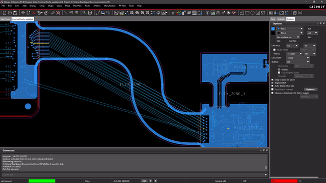
Another autorouter variation is what is known as an auto-interactive router. This tool still uses PCB autorouter technology, but gives interactive control to the designers to organize the nets and direct their path. To use auto-interactive routing in design systems like Cadence’s Allegro X PCB Editor, the designer first organizes the nets into bundles for maneuvering them as groups. The designer can edit the bundles to swap pins, assign board routing layers, or add net properties to help with maneuvering them as necessary. Once the bundles are positioned so as to work around congested areas, the designer can edit the bundles again to rearrange the net configuration to untangle pin connections and smooth the routing. Once the designer is satisfied with the routing pattern of the bundles developed in the virtual canvas, the autorouter will go to work and convert the bundles to routed traces.
With auto-interactive technology, PCB designers can direct the flow of their routing through high-density board designs with DDR or complex routing requirements. While a batch autorouter will connect every net on the board, it may not follow the paths or group the traces as precisely as a designer would prefer. Auto-interactive routing gives designers the precision control over the routing they need, while still providing the speed and precision of a traditional batch autorouter. With multiple variations and options of autorouting technology available to them in a single PCB CAD system, designers are fully equipped with the tools they need to get the job done. Next, we’ll look at a CAD tool that offers all of these features together in one system.
Cadence’s auto-interactive routing allows the design to group nets in bundles for organization
Autorouting in Cadence Allegro X
All of the PCB autorouting technology that we’ve discussed here is available in Cadence’s Allegro X PCB Editor. From the ability to simply route point-to-point single net connections to advanced auto-interactive routing, Allegro X has the autorouting capabilities you need as a designer. To complement the autorouting, Cadence’s Constraint Manager allows designers to easily assign design rules and constraints to nets and net classes, and components to govern parts placement. Designers will also be able to use the Constraint Manager to assign timing constraints and other electrical rules to their nets and set up constraints for fabrication and assembly.
Laying out a high-speed, high-density PCB design comes with a long list of challenges, and PCB designers need all the help they can get. With its different variations and options of PCB autorouting, Allegro X is the tool that can best serve your design needs.
For more information on high-speed designs that can benefit from the advantages of modern PCB autorouters, take a look at our Allegro X Design Platform product page.
If you’re looking to learn more about how Cadence has the solution for you, talk to our team of experts.