Using Current-Voltage Characteristics for Improved PCBA Design
Key Takeaways
-
What are the common types of current-voltage characteristics?
-
How are current-voltage characteristics used for PCBA design?
-
How to best utilize current-voltage characteristics during PCBA design.
Measuring current-voltage characteristics on a PCBA.
To some, it may seem that I took the scenic route to become an engineer. In retrospect, however, I think the time I spent as a technician not only provided a strong foundation in electronics that made the transition easier, but it also opened my eyes to what happens after the design stage. For some designs, it is obvious that the activities that occur downstream (such as manufacturing, testing, maintenance, and troubleshooting problems) were not considered during the design stage. And for others, well, the better ones are usually easy to identify due to the ease of subsequent tasks and lack of major problems.
The most important electrical parameters on a circuit board are the voltages, currents, and impedances. All other electrical values are derived or can be determined from these. When designing your PCBA, it is imperative to know what the input and output voltages and currents should be. However, there are other designs (for example, when there are on-board sources) where simply knowing the I/O is insufficient or inadequate. In these cases, a more comprehensive or improved design is required, and this objective can be achieved by effectively utilizing your board’s current-voltage characteristics, as we discuss in this article.
What Are Current-Voltage Characteristics?
Let’s begin with a definition:
A current-voltage characteristic, or I-V curve, illustrates the relationship between the current through a component, device, circuit, or system and the voltage across it. This characteristic provides a convenient means of evaluating the change in conductance (or inversely the impedance) of the element being analyzed.
As alluded to by the above definition, all electrical elements or systems can be characterized by a current-voltage characteristic. This usefulness is not lost on developers of products that utilize electricity. In fact, the I-V curve is an essential tool for designing and testing virtually all electronic and/or electrical systems, including those found on circuit boards.
How Are I-V Curves Typically Used during Circuit Board Design?
Good circuit boards begin with effective schematic design, and the most important decision made during this initial stage of board design is which components to use. In order to select the best components for design, it is imperative to have detailed operational data to make reasonable estimations of performance. The current-voltage characteristic is an important part of this data. Although necessary for passive electronic components, I-V curves are essential for evaluating active parts and devices such as op-amps and transistors, an example of which is shown in the figure below.
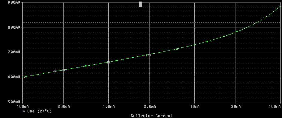
Example transistor I-V curve.
The use of I-V curves is a requirement for component selection when building your schematic, however, these analytical tools can also be utilized during the board layout phase, as discussed below.
How to Use Current-Voltage Characteristics to Improve Your PCBA Design
As stipulated in the definition above, I-V curves illustrate the level of conductance or impedance consistency of the element or system being analyzed. Therefore, these characteristics are one of the best tools for determining the range of I/O for elements and the PCBA, which can be used to ensure trace routes and connectors safely meet operational objectives. For high-power boards, designs where power supplies are on-board, and/or high-speed RF signals are propagated, the stackup materials and impedances become more important; specifically, choosing layer materials based on the dielectric constant, as shown below, to control board impedance is necessary.
PCB Stackup Layers Dielectric Specification.
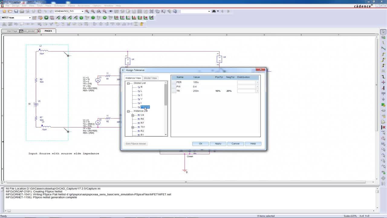
By utilizing the impedances determinable from I-V curves for routing traces and choosing stackup specifications, you can improve your board’s manufacturability and reliability. One of the best ways to evaluate current-voltage characteristics is by simulation, which requires that your PCB Design and Analysis package possesses this capability. The industry standard for Analog/Mixed-Signal Simulation is Cadence’s PSpice. With this tool, I-V curves for components, packages, devices, and boards can be easily analyzed, enabling you to achieve the best board design for your situation.
If you’re looking to learn more about how Cadence has the solution for you, talk to us and our team of experts.