How Using a Circuit Board Viewer Will Increase Your Design Group’s Efficiency
Key Takeaways
-
Some of the problems associated with traditional design review.
-
How everyone working with a circuit board viewer can be beneficial.
-
The truly great thing about working with a circuit board viewer.
Using a board viewer can help when putting your PCB under a microscope for review
It’s no secret that I like to eat, which is one of the more redeeming memories that I have of the PCB design review meetings that I used to attend. Don’t get me wrong, I completely agree with the purpose and benefits of a design review, but those old meetings used to be so long. They consisted of getting the documentation in order, distributing it, waiting for everyone to have a long look at it, and finally, lots of back and forth dialog. Those meetings could go on forever, but thankfully there was usually food available to help ease the pain a little.
Design reviews like that were not only tedious but they could also be less than thorough. Schematic or layout errors might not get caught, or new errors might be introduced due to multiple markups and corrections. Thankfully, the introduction of the PCB design viewer has provided exactly what is needed to improve this process. If you are looking for a way to decrease your design cycle time while increasing your overall department efficiency, take a look at some of the benefits that a circuit board viewer can offer. The only thing that you will miss out on now will be the free food.
The Problems With the Traditional Design Review Process
As previously mentioned, the need for a design review, or multiple reviews, is absolutely essential. It is important to get everyone’s buy-in on what is going on with the design. If you aren’t already, you should consider reviews for the following:
-
Pre-design review: This will allow all participants to offer design input before it starts. It is important that all aspects of the circuit board be represented here including software, mechanical, electrical, layout, test, and manufacturing.
-
Schematic completion: This review doesn’t have to involve a lot of people, but those that understand what needs to be included in a full schematic should attend.
-
Critical component placement and routing: Here is where the initial placement of the board will be reviewed. You will want to make sure that high-speed signal paths are correctly laid out and that sensitive routing is where it should be.
-
Final layout review: This is when the entire design team needs to come together again to make sure that the board is correctly laid out and ready for manufacturing.
There can be other reviews as well, such as a bill of materials (BOM) review or a specific review for manufacturability, but these are the main ones that you should include in your board design process.
The problem with all of these reviews is how the information is presented to the participants in the review. For years this was handled with a mountain of paperwork including schematics, BOMs, board layer plots, and netlist and testpoint reports. The best thing, of course, was to distribute all of this information far enough ahead so that each participant was ready for the review, but often, this wasn’t the case. Sometimes, updated copies would be re-distributed if something had changed, but that could create new problems if all of your markups were on the original copies.
The use of data-video projectors helped the review process by allowing the participants to see the actual design data together from a single source. Even then, the ultimate problem of not having universal access to the design data remained and wouldn’t be solved until the circuit board viewer became widely used.
A circuit board viewer can help eliminate the overwhelming amount of paper schematics and layouts
How Working Together With a Circuit Board Viewer Application Can Help
The best solution for all participants in a design review is for everyone to have access to the design data at their own work station. This allows for individual preparation before everyone gathers for the review, which cuts down on time spent in meetings. Electrical and layout engineers have always had access to their design software, but everyone else was usually without the means to review the data on their own. Here is where circuit board viewing software can really help.
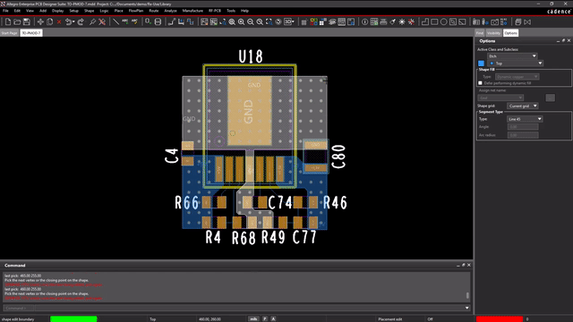
A good viewer application will allow the user to look at both the schematic and the layout of a circuit board without having to install the actual design tools. These viewers will give their users a way to mark up areas that need to be examined and create prints and plots if necessary. Many of these viewers will also allow communication between design team members so that changes can be easily passed around. And, the best tools contain advanced features such as measuring distances between design objects and the ability to select an object in the schematic and have it highlighted in the layout.
Viewers like this can make a big difference in how your team works together and performs design reviews. No longer do you have to wade through mountains of paperwork and cumbersome plots and prints that may or may not be the latest version of the project. Now, you can simply view the design files at your own workstation in order to be prepared for the design review. But there’s still more good news about these viewers.
A circuit board layout and schematic viewer will make your design reviews more efficient
The Best Part of Board Viewers
While circuit board viewers like this don’t allow you to make actual design changes, they do allow you to view and mark up the design for the engineers to correct later. The really great thing is that these viewers are often offered for free. Yes, that’s right, for free. EDA tool vendors will complement their design software with these free viewers in order to help design teams like yours work more efficiently together.
Free CAD viewers have been especially helpful during the work-at-home requirements imposed by the recent outbreak of COVID-19. Your extended design team can continue their work at home by reviewing the design on a viewer and sending in their comments for corrections or enhancements. The important part of all of this is to partner with a PCB design software company that has the top-of-the-line tools already so that the free viewer compliments your entire workflow.
The OrCAD line of PCB design tools from Cadence is an example of a PCB design system that includes a free viewer as part of its overall design package. With OrCAD PCB Designer, you will have access to a lot more than just PCB place and route. OrCAD has a complete suite of tools, including access to libraries, schematic capture, and SPICE tools, as well as all of the PCB layout features that you need.
If you’re looking to learn more about how Cadence has the solution for you, talk to us and our team of experts.