Home
Free Trial
Home
Free Trial
Read More
Content
Filter
10 results found
Featured
PCB Impedance Calculator: Trace Characteristics
Featured
An Overview of Circuit Routing Methodologies
Featured
Common Dielectric Waveguide Applications
Featured
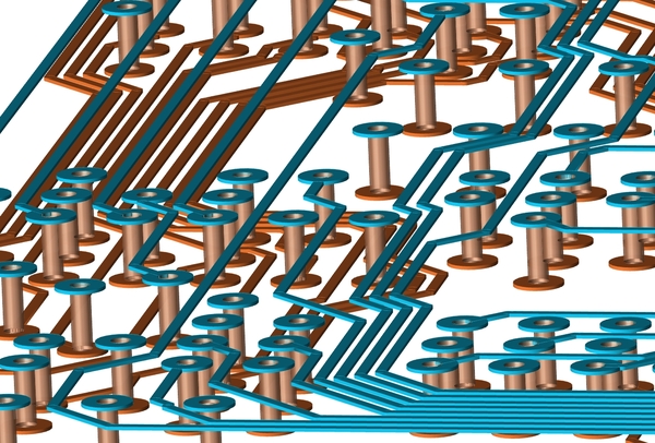
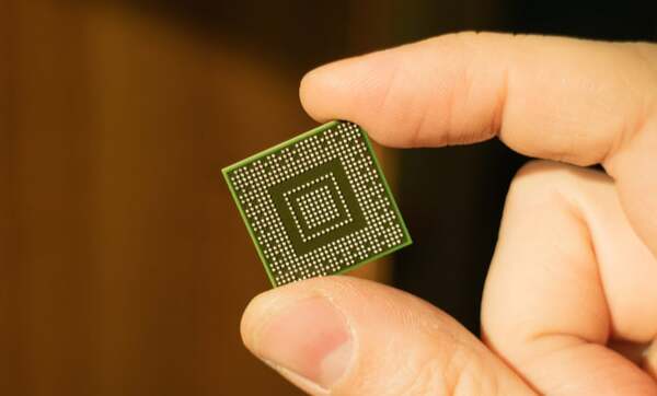
What Causes BGA Crosstalk?
Featured
Near-End Far-End Interference in Mobile Communication Systems
Featured
The Importance of RF Interference Shielding
Featured
Simplify Crosstalk Measurements and Mitigation Using Crosstalk Analysis
Featured
Crosstalk in Automotive Networking
Featured
The Impact of RF Shielding Effectiveness on Interference Mitigation
Featured
Anechoic Chamber RF Testing for Electromagnetic Compliance
Featured
Products
None
Content types
None
Blog
(10)
Solutions
None
Data & Process Management
(1)
PCB Layout
(1)
Simulation & Analysis
(7)
Design for Reliability
(1)