PCB Post-Layout Simulation While You Design
Key Takeaways
-
What is PCB post-layout simulation?
-
Different types of simulations that designers can run within the layout environment.
-
How a complete PCB design system with post-layout simulation can help.
Typical trace routing on a printed circuit board
The goal of electronics manufacturers is to design and build high-quality new products as quickly as possible to get them to market ahead of the competition. However, the traditional design workflow of building working prototypes to test a circuit board’s functionality can multiply the development schedule many times over. In contrast, simulation of a circuit board’s functionality can speed up the design cycle by a great amount, with the added benefit of improving the overall quality of the design.
PCB design simulators can be organized into two groups; those that simulate circuits to be designed and those that analyze circuits after they have been designed. With the performance requirements of today’s high-speed designs, the use of these simulators has become a regular and necessary part of the electronics development process. Fortunately, these tools are becoming easier to use and have found their way into the standard PCB layout process. Here is a closer look at PCB post-layout simulation and how it can benefit designers during their next design.
PCB Design Simulators
Today, complex circuit boards are rarely designed without the help of design simulation. Many different types and brands of simulators are available, with some operating as stand-alone tools, while others are incorporated into complete PCB design systems.
Design simulators can be divided between pre and post-layout tools, with the pre-layout simulators creating the parameters to be used in developing the design. This leaves the job of validating the design’s adherence to those parameters up to the post-layout simulators. Pre-layout simulators, such as SPICE tools (Simulation Program with Integrated Circuit Emphasis), evaluate circuitry logic in the schematic. In contrast, post-layout simulators or analysis tools are run against the completed physical layout.
Simulators rely on connectivity input from the design, as well as component and circuit models, for their calculations. Post-layout simulators will also extract physical elements from the routed board to make their calculations. These elements include traces, vias, metal area fills and planes as well as other board-level physical information necessary for calculations, such as dielectric material types, widths, and constants. All of this information is used to develop the simulation database to report their findings back to the designer.
The Benefits of PCB Post-Layout Simulation During Design
Post-layout simulation used to be a much more complex process than it is today. Originally, PCB layout information would have to be exported to a stand-alone analysis system that required a signal integrity expert to interpret the data. This process consumed a lot of time while the layout team waited for the results they needed. Thankfully, many simulators have now been simplified in their use and incorporated into standard PCB layout systems where they can give immediate feedback to circuit board designers.
Post-layout simulation can now be run by the layout team during the place and route phase of their design. Online analysis like this shortens the design cycle by giving immediate feedback to the design team about any signal integrity problems encountered while laying it out. Design teams can now route a bus of traces and then analyze that routing with the simulator to determine if it delivers the expected signal integrity. If not, the simulators will display graphical indications on the board layout showing which traces need to be adjusted to correct the problem.
Next, let’s take a look at some of the PCB layout-based simulators available and see how they can help designers.
Circuit Board Layout Simulators
The productivity of PCB layout designers is greatly enhanced by having simulation results at their fingertips. Here are some of the simulations that designers can now run during layout.
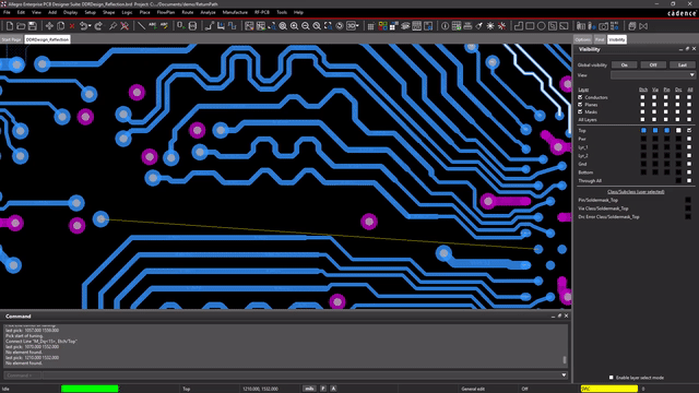
Signal Return Paths
It is essential to create clear signal return paths on the reference planes of high-speed PCB designs. Return paths that are blocked due to dense areas of vias, board features such as cutouts and slots, or even split planes can cause signal returns to wander around the board. These wandering return paths invariably create significant noise and EMI as they go. Noise and interference from signal path problems are one of the major sources of signal integrity problems and can easily degrade the functionality of circuits.
With PCB layout-based return path simulation, designers can quickly spot problems between a targeted signal and its return path. The results are clearly displayed on the layout, giving the designer the choice of how best to resolve the problem, as shown in the video below.
PCB post-layout simulation of signal return paths
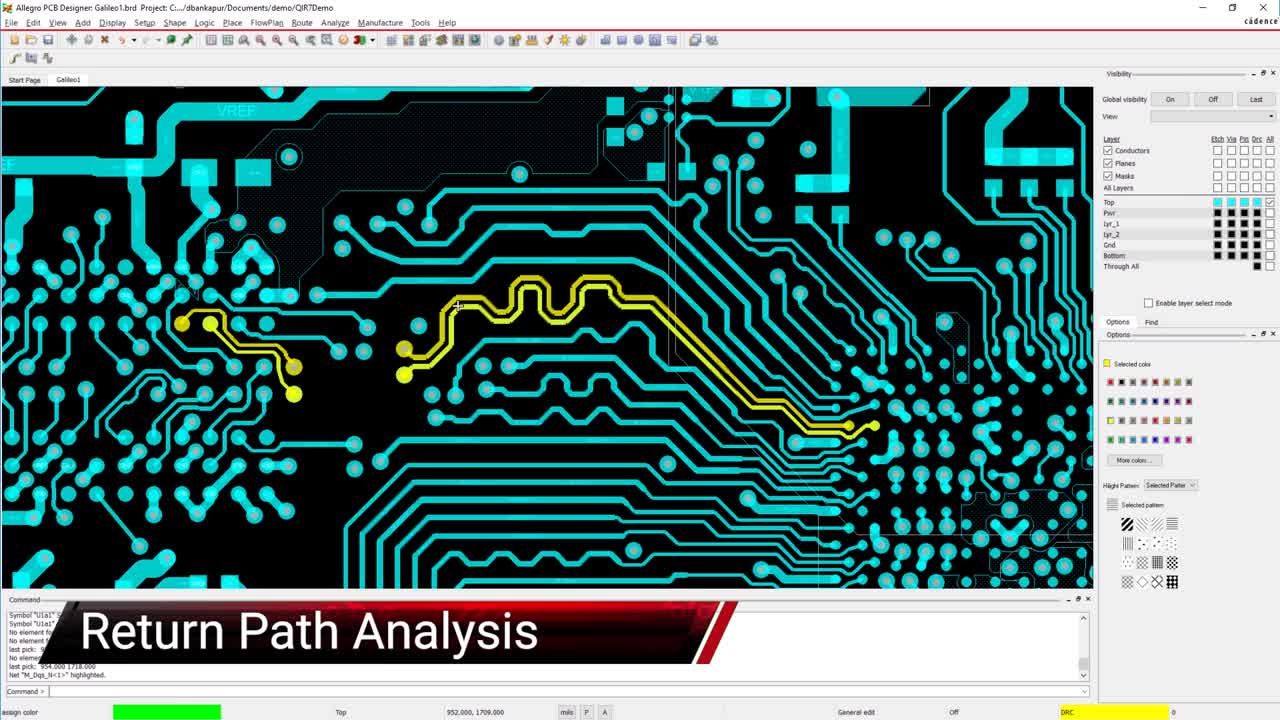
Coupling
Sensitive signals routed too close to other nets may be victimized by a stronger signal in a condition known as crosstalk. The aggressor signal may overpower a weaker signal, causing it to mimic the behavior of the stronger signal. Even though the spacing between the traces may be enough to satisfy the manufacturing requirements of the board, it may not be sufficient to prevent the unintentional electromagnetic coupling between them. Additionally, not only can crosstalk occur between traces routed side-by-side, but it can also happen between parallel traces running on adjacent layers of the board.
In the past, resolving problems like crosstalk relied on designers taking a lot of time running stand-alone analysis tools or debugging a prototype circuit board. Now, with post-layout simulations tools like the one shown below, coupling problems can be easily diagnosed and corrected while the board is still being laid out.
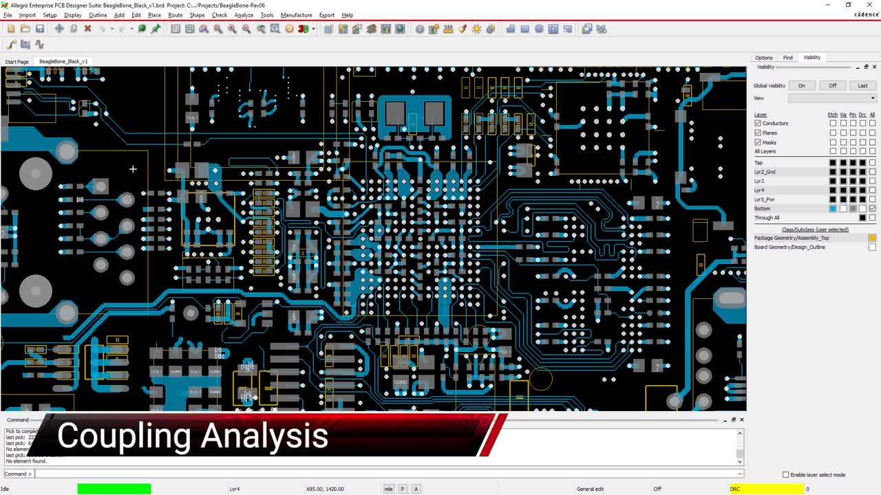
PCB post-layout simulation of unintentional trace coupling
Impedance
Impedance control requires precise calculations and carefully balancing the dielectric materials, the board layer stackup, and the width and spacing of impedance-controlled traces. While these steps allow designers to configure the design database for the best impedance conditions, it doesn’t allow designers to manage real-time impedance values. Without this control, impedance imbalances can lead to multiple signal integrity problems in a PCB design.
However, with post-layout simulation capabilities built into their design tools, PCB designers now have the capabilities they need to monitor their impedance-controlled traces during routing. As shown below, the simulator will display impedance discontinuities in traces by color-coding segments that are above or below the target impedance values. With this level of checking, design teams no longer need to wait until a prototype has been built to validate their work.
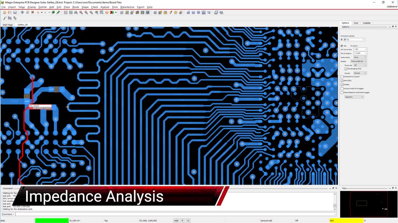
PCB post-layout simulation of trace impedance values
Reflection
One of the problems caused by mismatched impedance values in sensitive trace routing is signal reflection. High-speed signals in PCB designs rely on clear transmission and reception between their drivers and receivers. However, if the traces for these lines have varying impedances throughout their lengths, the signal can get reflected. This reflection can superimpose itself on the outgoing signal and distort it to the point where its profile is changed, degrading its integrity.
With PCB post-layout simulation tools like the reflection analysis workflow, shown below in the Allegro PCB Editor, designers can immediately evaluate signal reflection in their trace routing. The onscreen highlighted errors allow the layout team to find signal reflections and alter their design to avoid signal integrity problems.
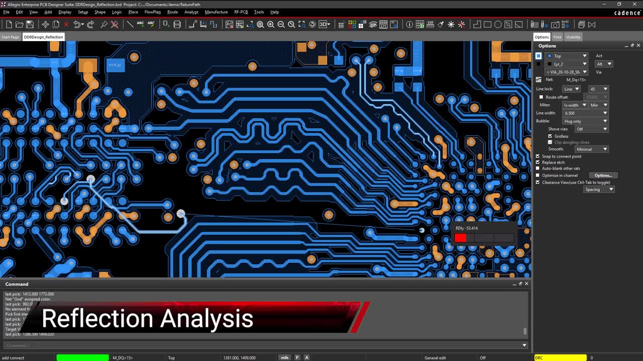
PCB post-layout simulation of signal reflections
Timing
The success of DDR and other high-speed routing configurations depends on creating the right trace lengths to support the timing requirements of the routing. At one time, PCB layout designers worked with reports and other line measuring tools to achieve the timing constraints they needed.
Now, with post-layout simulators that display timing results, as shown below, designers can easily see from color-coded traces which traces are too long and which are too short. Along with the timing simulators, automatic trace tuning features can also help designers quickly route their designs with the most optimum trace lengths.
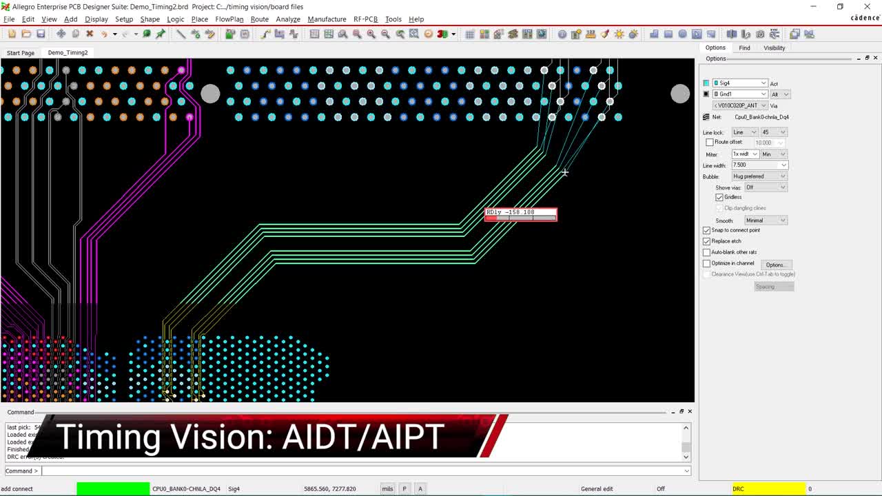
PCB post-layout simulation of high-speed trace routing timing
IR Drop
Creating a robust power delivery network (PDN) is essential for both power integrity and signal integrity in a printed circuit board design. However, it is very easy to miss tiny details such as critical power pins that aren’t receiving the voltage they need because of a thin connection to the power plane. Although the connection is enough to satisfy standard DRCs, it’s not enough to satisfy the power integrity requirements of the PDN.
PDN problems like these used to require the tedious debugging of a physical prototype. Now, power evaluations can be run quickly and efficiently during PCB layout by the design team. As shown below, the color-coded display will show where changes are needed to shore up the power or ground nets.
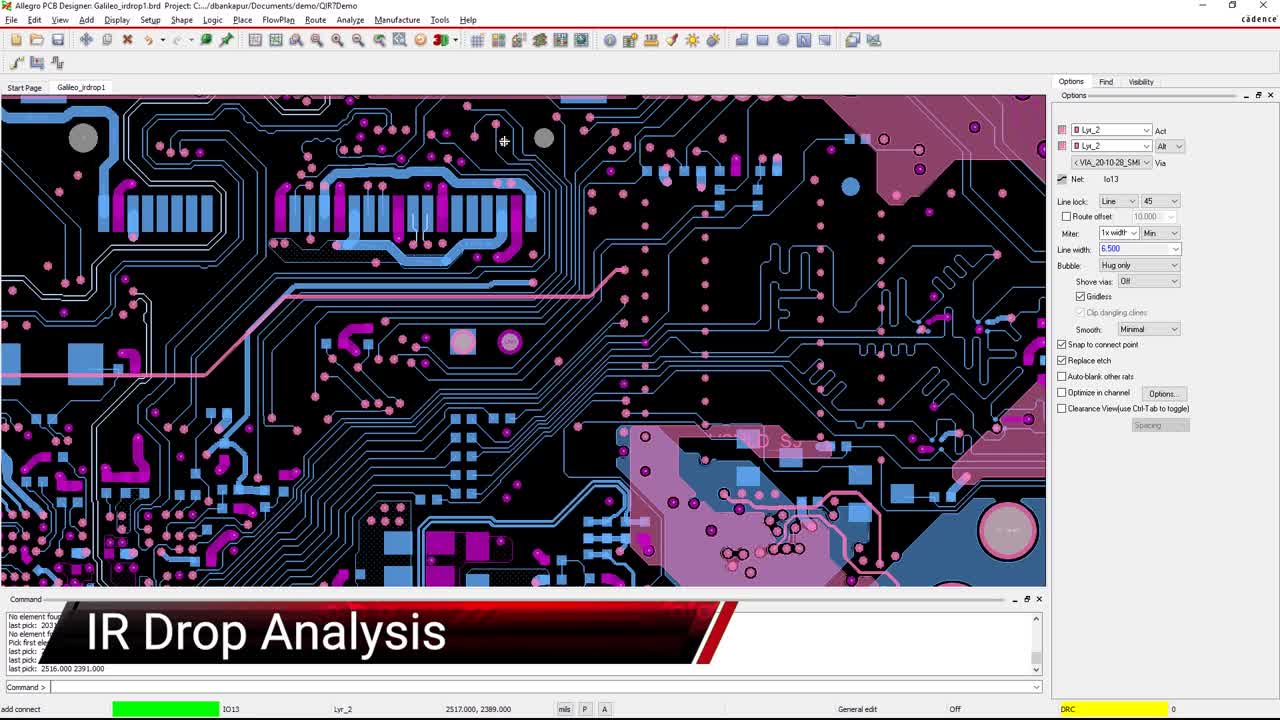
PCB post-layout simulation of a circuit board’s power delivery network
As we have shown, these PCB post-layout simulation tools can make a big difference in getting the design right the first time through. They can save time and money during the design cycle, and together with a complete PCB design system, make a designer’s job easier.
Essentials for the Complete PCB Design System
From schematic capture to the final documentation for manufacturing, PCB design CAD systems need a wide range of capabilities to get the job done. We’ve already seen the importance of using post-layout simulation tools during design, which is the backend of a complete simulation package, starting with an analysis of the circuitry during schematic capture. Additionally, a complete PCB design CAD package should have a comprehensive design rules and constraints system, multiple auto-routing capabilities, and 3D checking and viewing.
The Allegro X Design Platform by Cadence provides designers with these capabilities, enabling them to complete a wide range of designs, including analog, power, digital, flex, high-frequency, and more.
If you’re looking to learn more about how Cadence has the solution for you, talk to our team of experts.