17 - Waveform Analysis
Overview of waveform analysis
You can use the waveform analysis features of PSpice A/D to visually analyze and interactively manipulate the waveforms generated from the simulation data.
PSpice A/D uses high-resolution graphics so you can view the results of a simulation both on the screen and in printed form. On the screen, waveforms appear as plots displayed in Probe windows within the PSpice A/D workspace.
In effect, waveform analysis is a software oscilloscope. Performing a PSpice simulation corresponds to building or changing a breadboard, and performing waveform analysis corresponds to looking at the breadboard with an oscilloscope.
With waveform analysis you can:
- View simulation results in multiple Probe windows
- Compare simulation results from multiple circuit designs in a single Probe window
- Display simple voltages, currents, and noise data
- Display complex arithmetic expressions that use the basic measurements
- Display Fourier transforms of voltages and currents, or of arithmetic expressions involving voltages and currents
- For mixed analog/ digital simulations, display analog and digital waveforms simultaneously with a common time base
- Add text labels and other annotation symbols for clarification
PSpice A/D generates two forms of output: the simulation output file and the waveform data file. The calculations and results reported in the simulation output file act as an audit trail of the simulation. However, the graphical analysis of information in the waveform data file is the most informative and flexible method for evaluating simulation results.
Elements of a plot
A single plot consists of the analog (lower) area and the digital (upper) area.
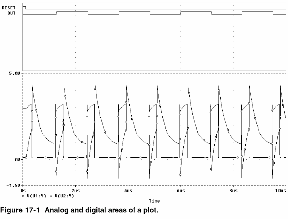
You can display multiple plots simultaneously. If you display only analog waveforms, the entire plot will be an analog area. Likewise, if you display only digital waveforms, the entire plot will be a digital area.
Elements of a Probe window
A Probe window is a separately managed waveform display area. A Probe window can include multiple analog and digital plots. Figure 17-2 shows two plots displayed together.
Because a Probe window is a window object, you can minimize and maximize windows, or move and scale the windows, within the PSpice A/D workspace. The toolbar in the Probe window applies to the active window.
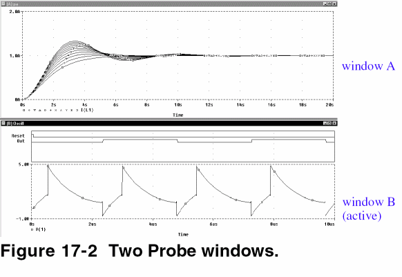
You can display information from one or more waveform data files in one Probe window. After the first file is loaded, you can load other files into the same Probe window by appending them in PSpice A/D (using the Append Waveform command under the File menu).
Managing multiple Probe windows
You can open any number of Probe windows. Each Probe window is a tab on the worksheet displayed in the middle of the workspace.
The same waveform data file can be displayed in more than one Probe window. You can tile the windows to compare data.
Only one Probe window is active at any given time. It is identified by a highlighted title bar or a topmost tab. Menu, keyboard, and mouse operations affect only the active Probe window. You can switch to another Probe window by clicking another tab or title bar.
Printing multiple windows
You can print all or selected Probe windows, with up to nine windows on a single page. When you choose Print from the File menu, a list of all open Probe windows appears. Each Probe window is identified by the unique identifier in parentheses in its title bar.
The arrangement of Probe windows on the page can be customized using the Page Setup dialog box. You can print in either portrait (vertical) or landscape (horizontal) orientation. You can also use Print Preview to view all of the Probe windows as they will appear when printed.
Toggling between display modes
You can choose from two different display modes in PSpice A/D: default and alternate.
The default display mode in PSpice A/D includes the main Probe window, plus the output window and the simulation status window. This provides all possible information about the simulation run and contains all of the toolbars and settings.
The alternate display mode shows only the Probe window with any waveforms that have been plotted. This mode gives you only the plots you are interested in seeing without the additional simulation data normally provided by PSpice A/D. By default, the alternate display mode is set to be visible at all times.
The toolbar and window settings are saved for each mode. Any changes you make in the settings will become the new default the next time you choose that display mode.
The alternate display mode can be very handy when you want to see the waveforms superimposed on the schematic diagram for easy debugging and testing of the circuit. You can customize the alternate display mode to view various toolbars or other PSpice A/D windows, according to your own preferences.
To toggle between the standard and the alternate display modes
- From the View menu, choose Alternate Display or click the Alternate Display toolbar button.
Keeping the Probe window visible at all times
Like any other application running under Windows, the PSpice A/D window will remain in the forefront of the desktop only as long as it is the active window. In order to keep the PSpice A/D window visible at all times, you can use the push pin feature.
By keeping the Probe window on top of other active windows, you can easily view the schematic page at the same time you see the corresponding waveform for that circuit. This allows you to cross-probe quickly and easily without having to activate the Probe window each time.
To make the Probe window visible at all times
- Click the push pin button in the toolbar.
Setting up waveform analysis
Setting up colors
- You can set the theme of the PSpice A/D application using the Probe Settings dialog box.
- You can configure the probe display using the Probe Settings dialog box or by editing the
PSpice.inifile. - You can configure the print colors only using the
PSpice.inifile.
For information on how to use the available colors and color order in a Probe window, see Configuring trace color schemes.
Setting application theme
- Choose Tools – Options.
The Probe Settings dialog box opens. - Click the Color Settings tab.
- Select
DarkorLightoption from the Application Theme drop-down list. - Click OK.
Editing display colors in the Probe Settings dialog box
- Choose Tools – Options to open the Probe Settings dialog box.
- Click the Color Settings tab.
- Select a background color from the Background list.
- Select a foreground color for the graph lines and texts from the Foreground list.
- Select the colors from the Available Colors list and click Add to add them to the Trace Colors list.
- Select a color in the Trace Colors list
- Click Up or Down to specify the order of the color.
- Click Remove to remove a color from the Trace Colors list.
The colors will be applied to traces in the sequence they are displayed. - Click OK.
You must restart PSpice A/D for the trace color changes.
Editing display and print colors in the PSpice.ini file
In the PSpice.ini file, you can control the following print and display color settings for probe windows:
- The colors used to display traces
- The colors used for the Probe window foreground and background
- The order colors are used to display traces
- The number of colors used to display traces
Editing the PSpice.ini file to modify display and print colors
PSpice.ini, you must restart PSpice A/D to ensure your changes take effect.- In a standard text editor (such as Notepad), open
PSpice.ini.
The default location ofPSpice.iniis:%HOME%\cdssetup\OrCAD_PSpice\<release_version>\PSpice.ini - Scroll to the
[PROBE DISPLAY COLORS]or[PROBE PRINTER COLORS]section of this file. - Add or modify a color entry. See Table 17-1 for a description of color entries and their default values. Colors for all items are specified as <item name>
=<color>.
The item names and what they represent are listed in Table 17-1. Valid item names include:- BACKGROUND
- FOREGROUND
- TRACE_1 through TRACE_12
black
blue
brightblue
brightcyan
brightgreen
brightmagenta
brightred
brightwhite
brightyellow
brown
cyan
darkblue
darkcyan
darkgray
darkgreen
darkmagenta
darkpink
darkred
green
lightblue
lightgray
lightgreen
magenta
mustard
orange
pink
purple
red
white
yellow
- If you added or deleted trace number entries, set
NUMTRACECOLORS=<n> to the new number of traces, where <n> is between 1 and 12. This item represents the number of trace colors displayed on the screen or printed before the color order repeats. - Save the file.
Table 17-1 Default waveform viewing colors
Item Name Description Default BACKGROUND
specifies the color of window background
BLACK
FOREGROUND
specifies the default color for items not explicitly specified
WHITE
TRACE_1
specifies the first color used for trace display
BRIGHTGREEN
TRACE_2
specifies the second color used for trace display
BRIGHTRED
TRACE_3
specifies the third color used for trace display
BRIGHTBLUE
TRACE_4
specifies the fourth color used for trace display
BRIGHTYELLOW
TRACE_5
specifies the fifth color used for trace display
BRIGHTMAGENTA
TRACE_6
specifies the sixth color used for trace display
BRIGHTCYAN
When you want to copy probe plots to the clipboard and paste them into a black and white document, do the following:
- Choose Window – Copy to Clipboard.
The Copy to Clipboard - Color Filter dialog box appears. - Choose change all colors to black in the Foreground section.
- Click OK.
Configuring trace color schemes
In the Probe Settings dialog box, you can set options for how the available colors and the color order specified in the PSpice.ini file are used to display the traces in a probe window. You can use:
- a different color for each trace
- the same color for all the traces that belong to the same y-axis
- the available colors in sequence for each y-axis
- the same color for all the traces that belong to the same waveform data file
For information on what the default available colors and color order are and how to change them, see Editing display and print colors in the PSpice.ini file.
To configure trace color schemes in the Probe Settings dialog box
- Choose Tools – Options to open the Probe Settings dialog box.
- Under Trace Color Scheme, choose one of the following options:
Table 17-2
Choose this option... To do this... Normal
Use a different color for each trace (for up to 12 traces, depending on the number of colors set in the
PSpice.inifile).Match Axis
Use the same color for all the traces that belong to the same y-axis. The title of the axis (by default, 1, 2, etc.) is the same color as its traces.
Sequential Per Axis
Use the available colors in sequence for each y-axis.
Unique by File
Use the same color for all the traces in one Probe window that belong to the same waveform data file.
- Click OK.
PSpice A/D saves the selected color scheme for future waveform analyses.
Viewing waveforms
If you are using one of the design entry tools, Capture or Design Entry HDL, you can either view waveforms automatically after you run a simulation, or you can monitor the progress of the simulation as it is running.
You do not need to exit PSpice A/D if you are finished examining the simulation results for one circuit and want to begin a new simulation from within the design entry tool. However, PSpice A/D unloads the old waveform data file for a circuit each time that you run a new simulation of the circuit. After the simulation is complete, the new or updated waveform data file is loaded for viewing.
Setting up waveform display from design entry tools
You can configure the way you want to view the waveforms in PSpice A/D by defining display settings in the Probe Window tab in the Simulation Settings dialog box.
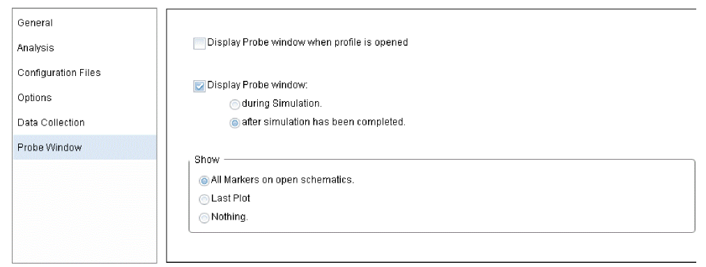
The display settings in the Probe Window tab are explained in the following table.
Table 17-3
| This setting... | Enables this type of waveform display... |
|---|---|
|
Display Probe window when profile is opened. |
Waveforms are displayed only when a .DAT file is opened from within PSpice A/D. |
|
Display Probe window... during simulation. |
Waveforms are displayed as the simulation progresses ("marching waveforms"). For digital data, marching waveforms are not supported.
|
|
Display Probe window... after simulation has completed. |
Waveforms are displayed only after the full simulation has completed and all data has been calculated. |
|
Show... All markers on open schematics. |
Waveforms are displayed for those nets that have markers attached in the schematic. |
|
Show... Last plot |
Waveforms are displayed according to the last display configuration that was used in the Probe window. |
|
Show... Nothing. |
No waveforms are displayed. |
Viewing waveforms while simulating
While a simulation is in progress, you can monitor the results for the data section being written by PSpice A/D. This function is only available when the Display Probe window during simulation option is enabled in the Probe Window tab of the Simulation Settings dialog box.
To monitor results during a simulation
- From the design entry tool’s PSpice menu, choose Edit Simulation Profile to display the Simulation Settings dialog box.
- Click the Probe Window tab.
- Select Display Probe window and then click during simulation.
- Click OK to close the Simulation Settings dialog box.
- From the PSpice menu, choose Run to start the simulation.
One Probe window is displayed in monitor mode.
If you open a new Probe window (from the Window menu, choose New Window) while monitoring the data, the new window also starts in monitor mode because it is associated with the same waveform data file.During a multi-run simulation (such as Monte Carlo, parametric, or temperature), PSpice A/D displays only the data for the most recent run in the Probe window. - Do one of the following to select the waveforms to be monitored:
- From PSpice A/D’s Trace menu, choose Add, and enter one or more trace expressions.
- From Capture’s PSpice menu, point to Markers, then choose and place one or more markers. Similarly, from Design Entry HDL’s PSpice Simulator menu point to Probes and choose and place one or more probes.
For more information, see Using schematic page markers to add traces.
Configuring update intervals
You can define the frequency at which PSpice A/D updates the waveform display as follows:
- At fixed time intervals (every n sec)
- According to the percentage of simulation completed (every n %), where n is user-defined
The default setting (Auto) updates traces each time PSpice A/D gets new data from a simulation.
To change the update interval
- From the Tools menu, choose Options.
- In the Auto-Update Interval frame, choose the interval type (sec or %), then type the interval in the text box.
Interacting with waveform analysis during simulation
The functions that change the x-axis domain (that set a new x-axis variable) can not be accessed while the simulation is running. If you have enabled the display of waveforms during simulation and wish to reconfigure the x-axis settings (as explained below), you must wait until the simulation run has finished.
The following table shows how to enable the functions that change the x-axis domain.
| Enable this function... | By doing this... |
|---|---|
|
Fast Fourier transforms |
|
|
Performance analysis |
|
|
New x-axis variable |
|
|
Measurement evaluation |
|
|
Load a completed data section |
|
Pausing a simulation and viewing waveforms
You can pause a simulation to analyze waveforms before the simulation is finished. After you pause the simulation, you can either resume the simulation or end it.
To pause a simulation
- From PSpice A/D’s Simulation menu, choose Pause.
- In the Probe window, view the waveforms generated before you paused the simulation.
- Do one of the following:
- From the Simulation menu, choose Run to resume the simulation.
- From the Simulation menu, choose Stop to stop the simulation.
Using schematic page markers to add traces
You can place markers on a schematic page to identify the nodes for which you want waveforms displayed in Probe. See Trace expressions for ways to add traces within PSpice A/D.
You can place markers:
- Before simulation, to limit results written to the waveform data file and automatically display those traces in PSpice A/D.
- During or after simulation, with PSpice A/D running, to automatically display traces in the active Probe window.
After simulation, the color of the marker you place is the same as its corresponding waveform analysis trace. If you change the color of the trace, the color of the marker on the schematic page changes accordingly.
The Markers submenu also provides options for controlling the display of marked results in PSpice A/D, after initial marker placement, and during or after simulation.
Power markers allow you to measure the power dissipation of a particular device. You can use these markers in the same way you use current and voltage markers. Power markers are annotated with "W" and are placed on devices that have PSpice models. The corresponding power dissipation waveforms for the devices will be calculated and displayed in Probe.
Place markers on subcircuit nodes. This allows you to perform cross-probing between the front-end design entry tool and PSpice A/D at the lower level circuits of a hierarchical design.
To place markers on a schematic page
- From Capture’s PSpice menu, point to Markers, then choose the marker type you want to place. Similarly, from Design Entry HDL’s PSpice Simulator menu, point to Probes, then choose the probe type you want to place (Some of the markers are from the Advanced submenu.)
Table 17-5
Waveform Markers/Probes menu command Advanced submenu command voltage

Voltage Level
not required
voltage
differentialVoltage Differential
not required
current

Current Into Pin
not required
digital signal
Voltage Level
not required
dB
Advanced
db Magnitude of Voltage
db Magnitude of Currentphase1
Advanced
Phase of Voltage
Phase of Currentgroup delay1
Advanced
Group Delay of Voltage
Group Delay of Currentreal1
Advanced
Real Part of Voltage
Real Part of Currentimaginary1
Advanced
Imaginary Part of Voltage
Imaginary Part of Currentpower
Power Dissipation
not required
- Point to the wires or pins you wish to mark and click to place the chosen markers.
- Right-click and select End Mode to stop placing markers.
- If you have not simulated the circuit yet, from the PSpice menu, choose Run.
After simulation, the color of the marker is the same as its corresponding waveform analysis trace. If you change the color of the trace, the color of the marker changes accordingly.
To hide or delete marked results
- From Capture’s PSpice menu, point to Markers, then choose one of the following:
Table 17-6
Choose this option... To do this... Hide All
Hide traces in the waveform analysis display for all markers placed on any page or level of the schematic.
Delete All
Remove all markers from the schematic and all corresponding traces from the waveform analysis display.
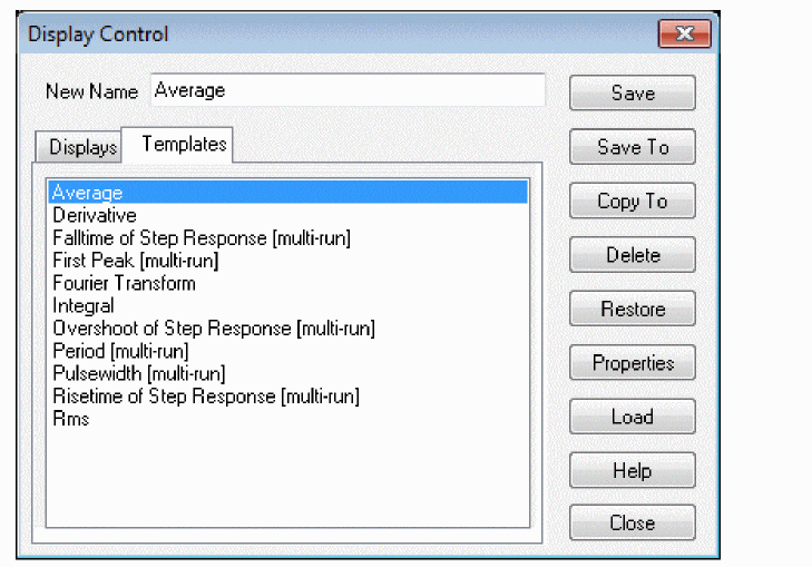
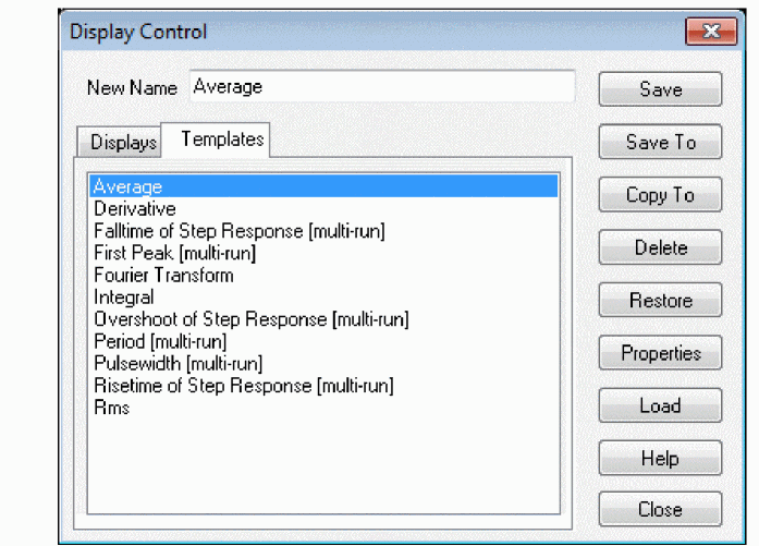
Using display control
You can create displays to save the contents of a Probe window. You can view a display again at a later time with a different simulation so long as the new simulation has identically named variables.
Once the display is saved, you can copy it, edit it, and delete it.
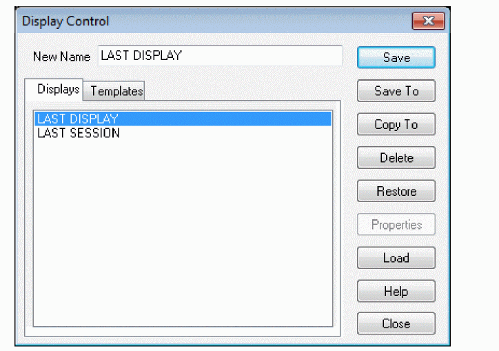
To save a display
- Set up the plots, traces, labels, and axes in the Probe window you want to save.
- From the Window menu, choose Display Control.
The Display Control dialog box appears. - Click on the Displays tab.
- In the New Name text box, type a name for the display.
- Do one of the following:
- To save the display in the current .PRB file, click Save.
- To save the display in another .PRB file, click Save To. Specify the name and location of the file. Click OK.
- Click Close.
To copy a display
- From the Window menu, choose Display Control.
The Display Control dialog box appears. - Click on the Displays tab.
- Click the name of the display to copy.
- Click Copy To.
- Specify the name and location of the copied display.
- Click OK.
- Click Close.
To delete a display
- From the Window menu, choose Display Control.
The Display Control dialog box appears. - Click on the Displays tab.
- Do one of the following:
- To delete a display from the current .PRB file, click the name, then click Delete.
- To delete a display from a global or remote .PRB file, click Delete From, then select the .PRB file.
- Click Close.
To use a saved display
- From the Window menu, choose Display Control.
The Display Control dialog box appears. - Click on the Displays tab.
- Do one of the following:
- To use a display listed here, click the name.
- To use a display from another .PRB, click Load. Select the file. Click OK. Click the name of the display.
- Click Restore.
To load displays from another .PRB file
- From the Window menu, choose Display Control.
The Display Control dialog box appears. - Click on the Displays tab.
- Click Load.
- Select the file.
- Click OK.
Using plot window templates
PSpice A/D provides plot window templates that allow you to create and reuse custom displays in Probe using defined arguments. A plot window template is a plot window consisting of one or more arguments used to represent node voltage, pin current, power or digital names within a display. An argument provides the means to replace a fixed node voltage or pin current name with a node voltage or pin current name you choose.
You can create unique plot window templates for a particular design or general templates that can be applied to various designs. A set of some of the more commonly used templates are predefined and included with PSpice A/D.
To work with plot window templates, from the Window menu, choose Display Control, and click the Templates tab. Here you can customize plot window templates in various ways.
Creating a plot window template
In order to create and save a new plot window template, you must first set up the active plot window in Probe with the configuration you want. The active plot window will be the basis for the template properties you save.
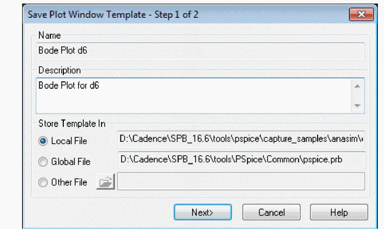
To create a new plot window template
- In PSpice A/D, from the Window menu, choose Display Control.
- Click the Templates tab.
- In the New Name text box, enter the name for the new template you want to create.
- Click Save or Save To.
The Save Plot Window Template – Step 1 of 2 dialog box appears.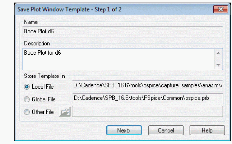
- In the Description text box, type in a description for the template, if you would like one. (This is optional.)
- If you clicked Save To, choose the .PRB file you wish to save the template to by selecting the appropriate radio button under the Save Template In frame. (The default is the local .PRB file. For the Save function, the Local File is the only option.)
- Local File – the .PRB file for the current simulation in PSpice A/D.
- Global File – the .PRB file to be used globally for all Probe displays.
- Other File – another .PRB file stored elsewhere on your hard disk or network drive. Use the Browse button to locate the file on a particular drive.
- Click the Next> button.
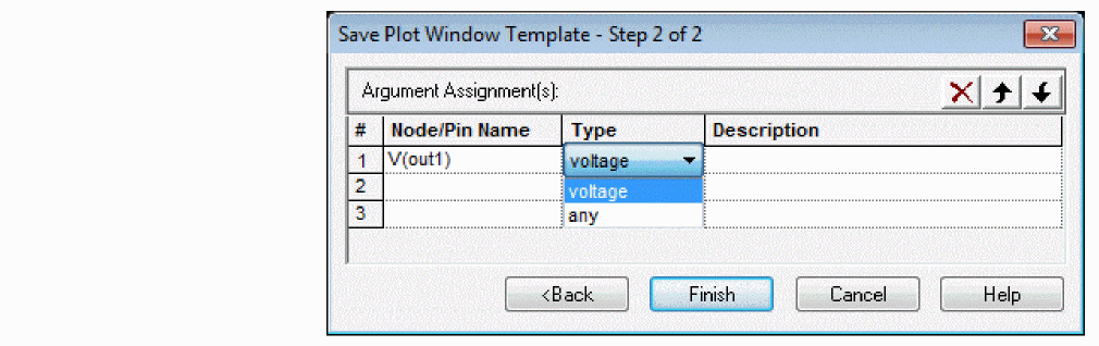
The Save Plot Window Template – Step 2 of 2 dialog box appears. The number of Node/Pin Name arguments that are listed here is determined by the current display.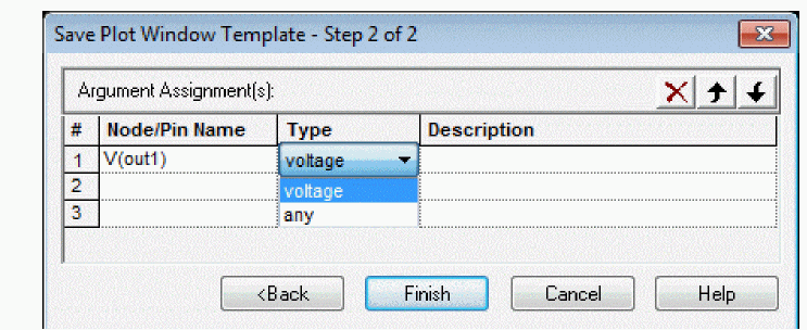
- Define the association of each argument by selecting the node or pin name from the drop-down list under the column Node/Pin Name.
This drop-down list shows all of the available node voltage, pin current, power or digital names. If the drop-down list does not appear, click in the text box to activate the drop-down button. - For each argument, set the Type of argument to be used by selecting the argument name from the drop-down list under the column Type.
This drop-down list shows all of the available argument types (any, current, power, voltage). If the drop-down list does not appear, click in the text box to activate the drop-down button. - For each argument, under the Description column, type in a description for the argument, if you would like one. (This is optional.)
The description you enter here will be displayed in the status line of Capture when placing a marker associated with the argument. - If desired, change the order of the arguments by using the Arrow buttons to move an argument up or down in the listing. Or, you can delete an argument by selecting it and clicking the Delete button.
- Click Finish.
Modifying a plot window template
Modifying a plot window template is essentially the same as creating a new template. In order to modify a plot window template, that particular template must be the active plot window in Probe. If the active display is not the template you want to modify, use the Restore button to make a different template the active display in Probe
To modify a plot window template
- From the Window menu, choose Display Control.
- Click the Templates tab.
- Select the template you want to modify by clicking on its name in the list of loaded templates. If the template you are looking for is not in the list, use the Restore button to make it the active display.
- Click the Save button to display the Save Plot Window Template – Step 1 of 2 dialog box.
- Make the desired changes, then click Next to display the Save Plot Window Template – Step 2 of 2 dialog box.
- Make the desired changes, then click Finish.
The modifications will be saved and the display will be updated automatically.
Deleting a plot window template
You can easily delete a plot window template from the list of loaded templates. This does not erase the template from your system. It only removes it from the list of templates you can access and erases it from the .PRB file.
To delete a plot window template
- From the Window menu, choose Display Control.
- Click the Templates tab.
- Click on the name of the plot window template you want to delete.
- Click Delete.
Copying a plot window template
You can copy a plot window template into another .PRB file to make it available for use later with that file.
To copy a plot window template
- From the Window menu, choose Display Control.
- Click the Templates tab.
- Click on the name of the plot window template you want to copy.
- Click Copy To.
The Probe File for Save Template dialog box appears. - Choose the .PRB file you wish to save the template to by selecting the appropriate radio button under the Save Template In frame. (The default is the local .PRB file.)
- Local File – the .PRB file for the current simulation in PSpice A/D.
- Global File – the .PRB file to be used globally for all Probe displays.
- Other File – another .PRB file stored elsewhere on your hard disk or network drive. Use the Browse button to locate the file on a particular drive.
- Click OK.
Restoring a plot window template
In order to make a plot window template the active display in Probe, you must restore it. This process recalls a previously defined plot window template and sets up a new plot window in Probe using the arguments associated with that template. In order for the arguments in the template to apply, you must replace the node voltage names or pin current names for each argument contained in the restored template.
To restore a plot window template
- From the Window menu, choose Display Control.
- Click the Templates tab.
- Click Restore.
The Restore Plot Window Template dialog box appears.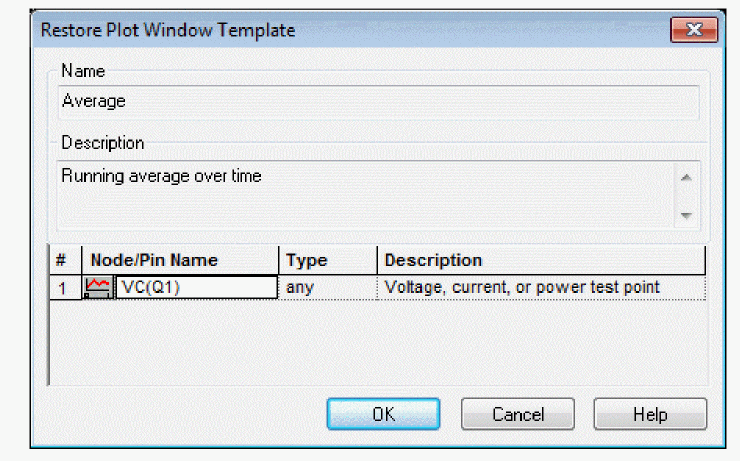
- Reassign the node voltage names or pin current names for each argument in the list.
- Click OK.
A new Probe window will be created and the restored plot window template will be displayed.
Viewing the properties of a plot window template
You can view the properties of a plot window template and change the description fields for the template or arguments it contains.
To view the properties of a plot window template
- From the Window menu, choose Display Control.
- Click the Templates tab.
- Click on the name of the plot window template you want to view.
- Click Properties.
The Plot Window Template Properties dialog box appears.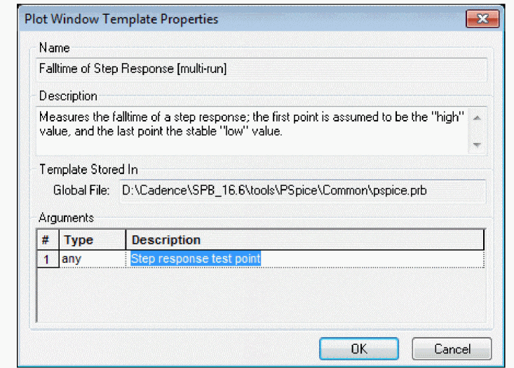
- Change the Description field for the template, or change the description for any of the Arguments, as desired.
- Click Finish to exit and save any changes.
Loading a plot window template
You can load a plot window template from another .PRB file, and add it to the list of available templates. When you load a template, you do not make it the active display in Probe. You are only adding it to the list of available templates. (To view the newly loaded template, you need to restore it.)
If a duplicate template is loaded, then the one you are loading will replace the current one in the list. If you close the data file and reopen it, any plot window templates that you loaded earlier will have to be loaded again to make them available. (Loaded templates are not saved with the data file.)
To load a plot window template
- From the Window menu, choose Display Control.
- Click the Templates tab.
- Click Load.
The Load Displays dialog box appears. - Locate the .PRB file that contains the plot window template you want to load.
- Select the file and then choose Open.
The loaded templates will be listed in the Display Control dialog box.
Placing plot window template markers in Capture
Place a marker in Capture that represents a plot window template. The marker will restore the associated template when you run the simulation in PSpice A/D. Markers for plot window templates are distinguished from other markers (for voltage, current, or power) by being square rather than round in shape.
A simulation profile must be active in order to place a marker for a plot window template. The analysis type defined in the profile will determine what type of template will be loaded (either for AC, DC or transient analysis).
When placing a plot window template marker, the argument description for the template being placed will appear in the status bar of Capture. Markers will continue to be placed until all arguments for the template have been satisfied. If an active simulation exists, then the template markers will turn black; otherwise, they will remain gray.
If an argument type is set to "Any" rather than a specific type, the marker type will depend on the marker placement location. If a marker is placed on a pin, then it will be assumed to be a current marker. If a marker is placed on a node, it will be assumed to be a voltage marker. If a marker is placed on a device, it will be assumed to be a power marker.
To place a plot window template marker
- In Capture, from the PSpice menu, choose Markers, then select Plot Window Templates.
The Plot Window Templates dialog box appears.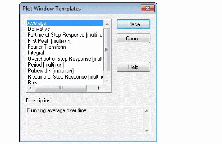
- Click on the template you want to associate with the marker you will place.
- Click the Place button.
A plot window template marker will appear and be attached to the cursor. - Place the marker at a particular location on the schematic page.
- Continue to place markers at the appropriate locations until all the arguments for the template have been satisfied.
Limiting waveform data file size
When PSpice A/D performs a simulation, it creates a waveform data file. The size of this file for a transient analysis is roughly equal to:
(# transistors)·(# simulation time points)·24 bytes
The size for other analysis types is about 2.5 times smaller. For long runs, especially transient runs, this can generate waveform data files that are several megabytes in size. Even if this does not cause a problem with disk space, large waveform data files take longer to read in and take longer to display traces on the screen.
You can limit waveform data file size by:
- placing markers on your schematic before simulation and having PSpice A/D restrict the saved data to these markers only
- excluding data for internal subcircuits
- suppressing simulation output
Limiting file size using markers
One reason that waveform data files are large is that, by default, PSpice A/D stores all net voltages and device currents for each step (for example, time or frequency points). However, if you have placed markers on your schematic prior to simulation, PSpice A/D can save only the results for the marked wires and pins.
To limit file size using markers
- From Capture’s PSpice menu, choose Edit Simulation Profile.
The Simulation Settings dialog box appears. - Click the Data Collection tab.
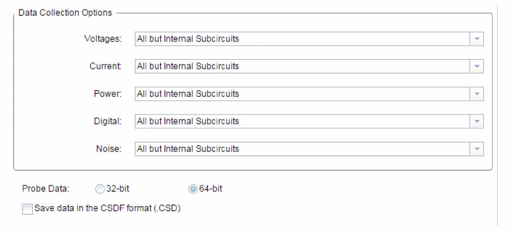
- In the Data Collection Options section, choose the desired option for each type of marker (Voltages, Current, Power, Digital, Noise).
Table 17-7
Option Description All
All data will be collected and stored. (This is the default setting.)
All but Internal Subcircuits
All data will be collected and stored except for internal subcircuits of hierarchical designs (top level data only).
At Markers only
Data will only be collected and stored where markers are placed.
None
No data will be collected.
- Check the Save data in the CSDF format (.CSD) if you want the data to be stored in this format.
By default, the probe data has an accuracy of 64-bit. You can change this to 32-bit. - Click OK.
- From the PSpice menu, select Markers, then choose the marker type you want to place.
The color of the marker on the schematic page is the same as its corresponding waveform analysis trace. If you change the color of the trace, the color of the marker changes accordingly. - Point to the wires or pins you wish to mark and click to place the chosen markers.
- Right-click and select End Mode to stop placing markers.
- From the PSpice menu, choose Run to start the simulation.
When the simulation is complete, the corresponding waveforms for the marked nodes or devices will be displayed in Probe.
Limiting file size by excluding internal subcircuit data
By default, PSpice A/D saves data for all internal nodes and devices in subcircuit models in a design. You can exclude data for internal subcircuit nodes and devices.
To limit file size by excluding data for internal subcircuits
- From the Capture’s PSpice menu, choose Edit Simulation Profile.
The Simulation Settings dialog box appears. - Click the Data Collection tab.
- In the Data Collection Options section, choose
All but Internal Subcircuitsfor each marker type. - Click OK.
- From the PSpice menu, choose Run to start the simulation.
Limiting file size by suppressing the first part of simulation output
Long transient simulations create large waveform data files because PSpice A/D stores many data points. You can suppress a part of the data from a transient run by setting the simulation analysis to start the output at a time later than 0. This does not affect the transient calculations themselves—these always start at time 0. This delay only suppresses the output for the first part of the simulation.
To limit file size by suppressing the first part of transient simulation output
- From Capture’s PSpice menu, choose Edit Simulation Profile to display the Simulation Settings dialog box.
- Click the Analysis tab.
- From the Analysis type list, select the Time Domain (Transient) option.
- In the Start saving data after text box, type a delay time.
- Click OK to close the Simulation Settings dialog box.
- From the PSpice menu, choose Run to start the simulation.
The simulation begins, but no data is stored until after the delay has elapsed.
Viewing large data files
At times there are situations where you cannot reduce the size of the data file being generated, but would like to load large data files on to the Probe for viewing the trace.
As PSpice A/D depends on system memory for loading and displaying any trace, if the data file is so large that cannot be loaded, the trace does not get displayed at all. Usually data files with size greater than 2 GB are considered to be large data files. Whether a data file can be categorized as large depends on the size of the data file and the number of traces within the data file. For example, a data file that has 10 traces and is of 2 GB may not be a large data file. But if a data file has single trace and is of 2 GB or more, it can be termed as a large data file.
Large data files are usually loaded faster compared to the smaller data files in terms of rate of loading. However, PSpice A/D provides options to optimize the loading and viewing of large data files. To load and view data files with more than 1 million data points, PSpice A/D provides you with the following options.
- Displaying fewer data points
- Displaying partial trace
Displaying fewer data points
If a data file is too large to be loaded on to PSpice A/D, you can choose to display the complete trace that has been created using a fewer data points.
For example, if the complete trace uses 3 million data points, the trace displayed on the probe window will be created using only 1 million data points.
In this option though the complete trace is displayed, it is not very accurate. The number of data points used to construct the complete trace depends on the system memory available for loading data points. By default, the limit is set to 1 million data points per part of the trace. If required you can increase this limit. For more information see, Changing threshold for large data file.
Displaying partial trace
Another method of loading and displaying a large data file on to PSpice, is to break the complete trace into multiple smaller parts. You can then view each part separately in the PSpice A/D probe window. See the figure below.
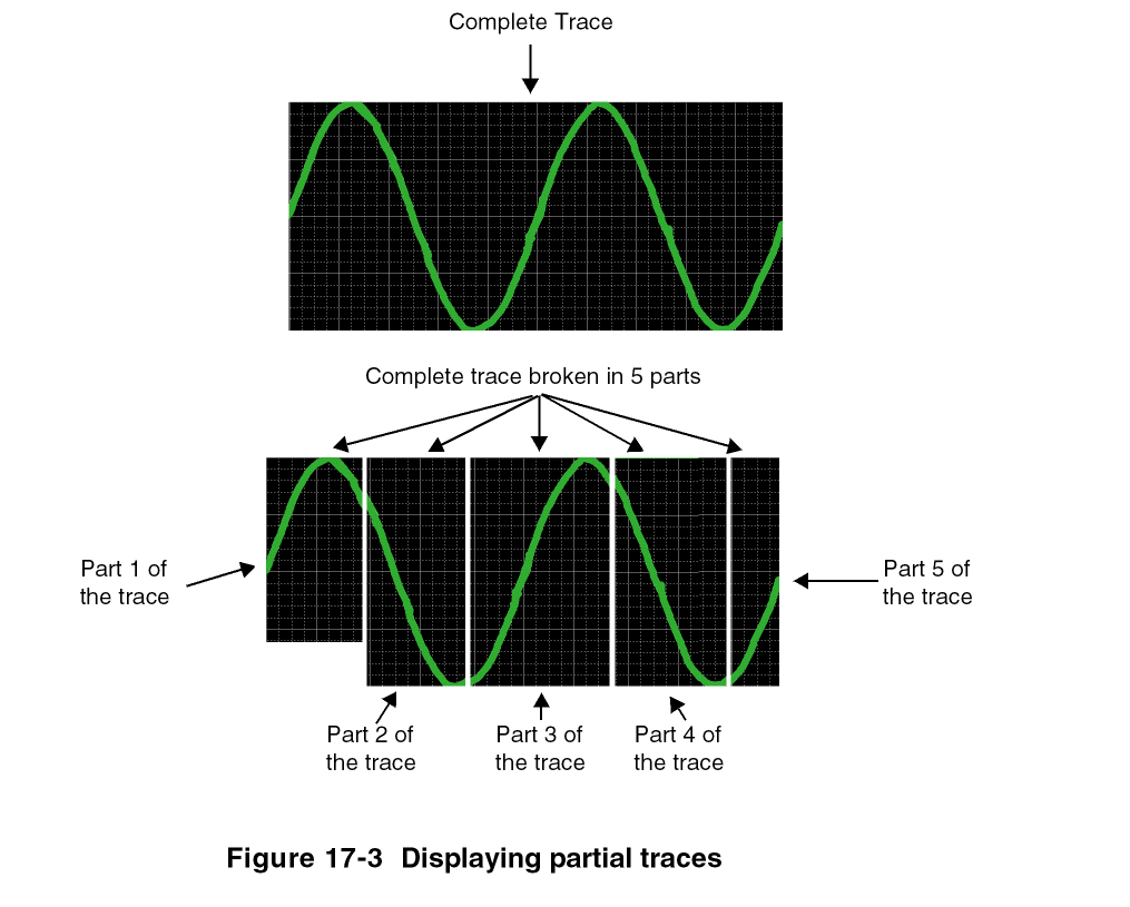
Number of parts into which the complete trace can be divided is governed by the number of data points in the trace.
For example, if a complete trace has 4.5 million data points, and at any given point of time PSpice A/D is configured to load only 1 million data points, the complete trace will be divided into 5 parts. First four part traces will be of 1 million data points each and the last part trace will be of 500000 data points.
The size of the partial trace is also influenced by the number of data points per part. By default, the limit is set to 1 million data points per part of the trace. If required you can increase this limit. For more information see, Changing threshold for large data file.
When you display partial traces, marching waveforms are not supported.
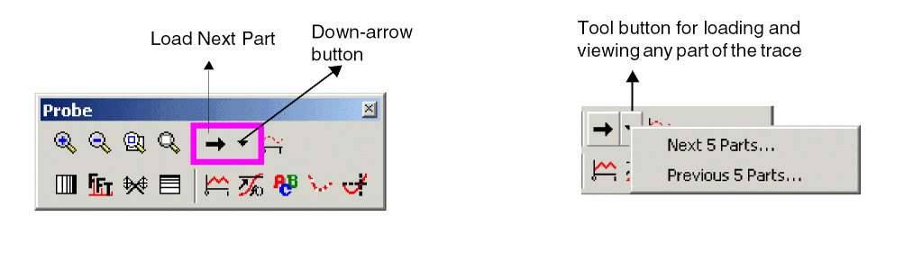
You can also use the Load Next Part button in the Probe toolbar for loading and viewing the next part of the trace. The down-arrow button is used to display the next 5 or the previous 5 parts of the trace or both as the case may be.
Loading a large data file
If you are trying to open a large data file in PSpice A/D, the Large Data File dialog box appears.
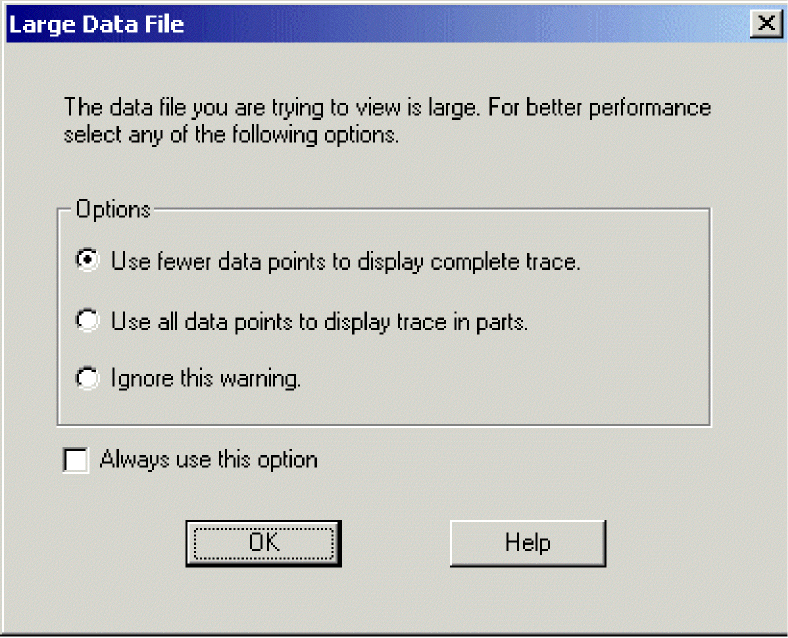
To load and display the data file, you can either select the Use fewer data points to display complete trace option or the Use all data points to display trace in parts option.
To load the complete data file, select the Ignore this warning option. When you select this option, the data file may or may not get loaded depending on your system memory.
For example, on some machines a data file with 5 million data points may open without any problems while on some other machine the same data file might be too large to be loaded in one go.
To make your selection the default setting, select the Always use this option check box. Once this check box is selected, next time when you try to open a large data file, the Large Data File dialog box does not appear. Instead, the option selected by you previously is used to open the large data file.
The following two options are disabled for marching waveforms:
- Use fewer data points to display complete trace
- Use all data points to display trace in parts
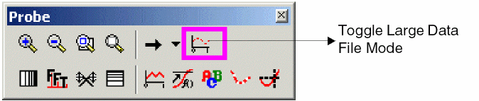
Switching Modes
While viewing the trace from a large data file, you can switch from one mode to another using one of the following methods.
- Using the View drop-down menu
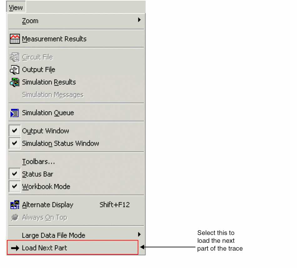
- From the View menu in PSpice A/D select Large Data File Mode.
- In the Large Data File Mode submenu, select the mode in which you want to view the trace. The mode currently selected, has a check mark against it.
- Select Display Fewer Data Points when you want to view the complete trace that may not be very accurate.
- Select Display in parts when you want to view the partial but an accurate representation of the trace.

- Using the toolbar
- To switch modes, select the Toggle Large Data File Mode button in the Probe toolbar.
- To switch modes, select the Toggle Large Data File Mode button in the Probe toolbar.
Changing threshold for large data file
By default, in PSpice A/D any data file with more than 1 million data points is categorized as a large data (.dat) file. As a user you can modify this threshold by specifying a higher the number of data points in the Probe Settings dialog box.
To increase the number of data points complete the following steps:
- From the Tools menu in PSpice A/D choose Options.
This option is enabled only if a.dator.simfile is open in PSpice A/D. - Select the Large Data File tab.
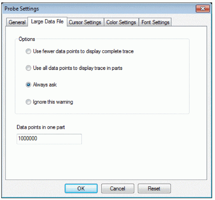
- In the Data points in one part text box specify the desired number of data points and click OK.
The changes you have made in the Probe Setting dialog box, will be effective from the next session.
Any changes to the threshold for defining large data file should be made keeping in account your system memory so as to avoid failure in opening data files. For example, on a machine low on system memory, a data file or a part of data file with 2 million data points might fail to open. On the other hand, for a high-end machine a limit of 3 million data points might work fine.
Using simulation data from multiple files
You can load simulation data from multiple files into the same Probe window by appending waveform data files.
When more than one waveform data file is loaded, you can add traces using all loaded data, data from only one file, or individual data sections from one or more files.
Appending waveform data files
To append a waveform data file
- In PSpice A/D, from the File menu, choose Append Waveform (.DAT).
- Select a *
.DATfile to append, and click OK. - If the file has multiple sections of data for the selected analysis type, the Available Sections dialog box appears. Do one of the following:
- Click the sections you want to use.
- Click the All button to use all sections.
- Click OK.
Importing traces
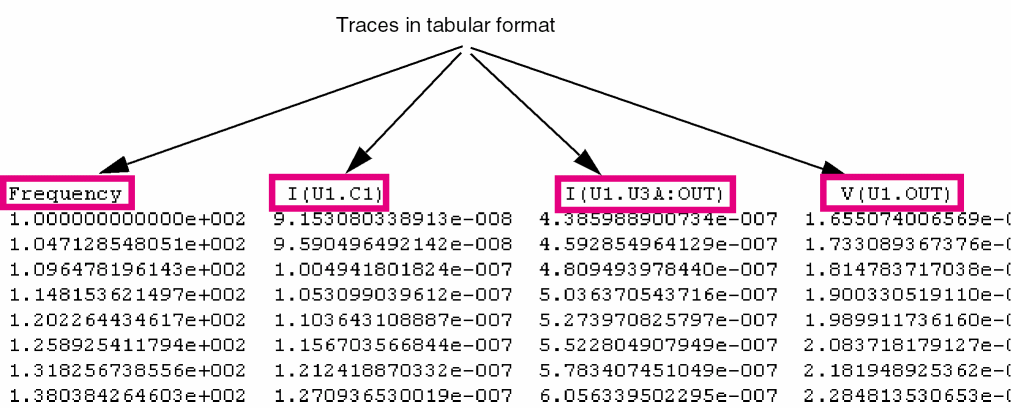
Besides using the simulation data from .DAT files, you can also import trace information stored in other file formats. Using PSpice A/D you can import the traces stored in a tabular format in a .txt file or a .csv file.
To import a trace
- From the File drop-down menu choose Import.
- In the Import File dialog box, select the text file to be imported in PSpice A/D.
The Import Traces dialog box appears. All the nodes listed in the source file are listed in the X-axis drop-down list and the Available Nodes list. - In the Import Traces dialog box, specify the name and the location of the .DAT file in which the imported trace is to be stored.
- From the X-Axis drop-down list box, select the node name to be plotted on the X-Axis.
- Specify a name for the X-axis. Select one of the following options for naming the X-axis.
- Time
- Frequency
- Sweep Variable: When you select Sweep Variable, you need to specify the variable name in the enabled text box.
- From the Available Traces list box, select the traces that are to be imported in PSpice A/D.
- Click Add.
- The selected traces appear in the Import Trace list box. To import all the traces available in the source file, click the Add All.
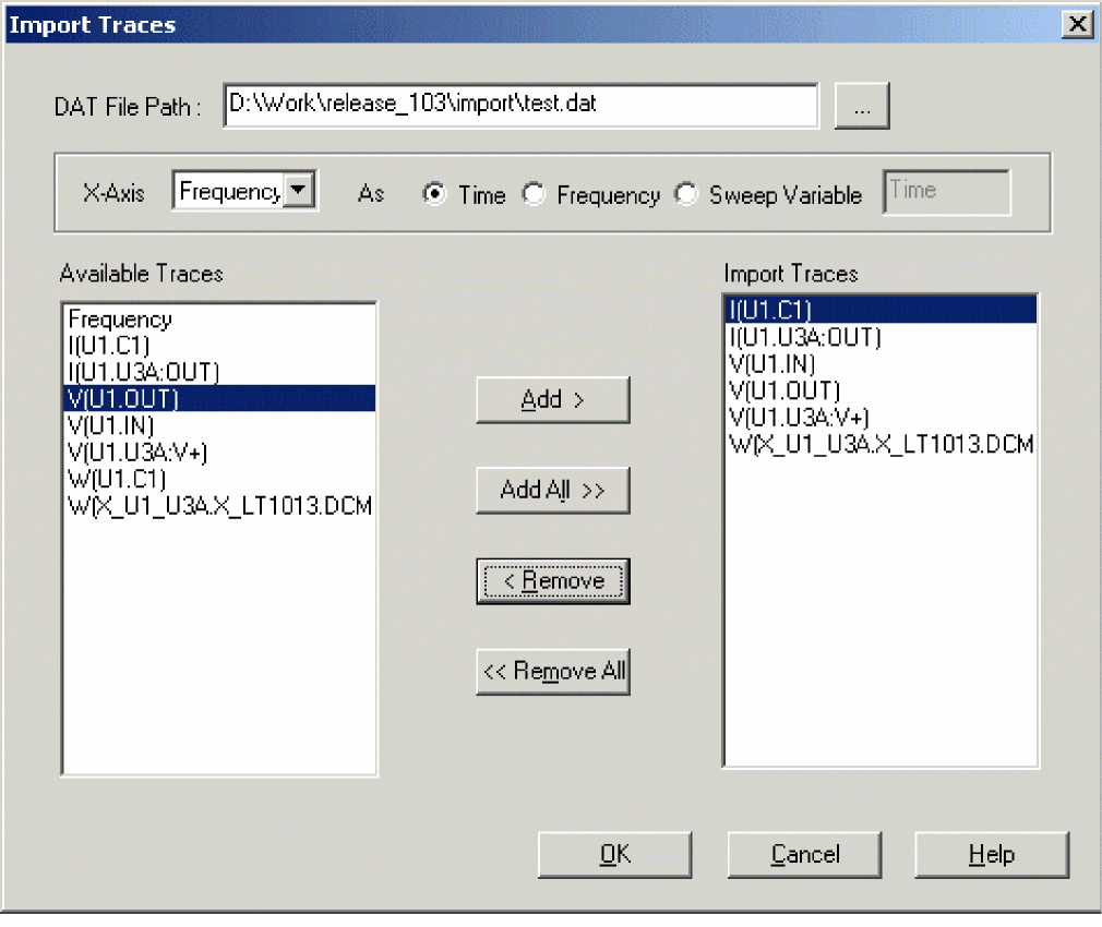
- Select OK to import the selected trace(s) into the specified data file.
Renaming of X-axis is useful when you want to import a trace and append it to an existing data file for comparing traces. To be able to append two traces successfully, you need to ensure that for both the traces the range and the name of the variable plotted on the X-axis should be same.
Adding traces from specific loaded waveform data files
If two or more waveform data files have identical simulation output variables, trace expressions that include those variables generate traces for each file. However, you can specify which waveform data file to use in the trace expression. You can also determine which waveform data file was used to generate a specific trace.
To add a trace from a specific loaded waveform data file
- In PSpice A/D, from the Trace menu, choose Add Trace to display the Add Traces dialog box.
The Simulation Output Variables list in the Add Traces dialog box contains the output variables for all loaded waveform data files. - In the Trace Expression text box, type an expression using the following syntax:
trace_expression@fn
where n is the numerical order (from left to right) of the waveform data file as it appears in the PSpice title bar, or
trace_expression@s@fn
where s is a specific data section of a specific waveform data file.
Example: To plot the V(1) output for data section 1 from the second data file loaded, type the following trace expression:V(1)@1@f2
You can also use the name of the loaded data file to specify it. For example, to plot the V(1) output for all data sections of a loaded data file, MYFILE.DAT, type the following trace expression:V(1)@"MYFILE.DAT"
- Click OK.
To identify the source file for an individual trace
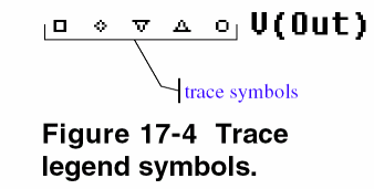
- In the trace legend, double-click the symbol for the trace you want to identify (Figure 17-4).
 The Section Information dialog box appears, containing the trace name and—if there is more than one waveform data file loaded in the plot—the full path for the file from which the trace was generated.
Also listed is information about the simulation that generated the waveform data file and the number of data points used (Figure 17-5).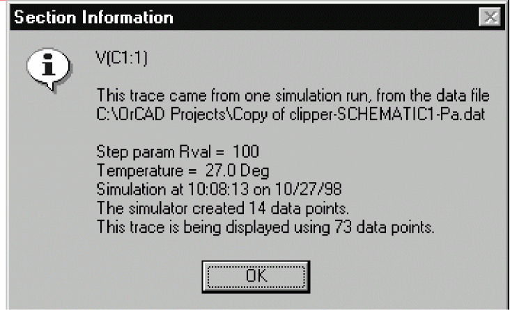 Figure 17-5 Section information message box.
Comparing measured data with simulated data
You can compare measured data with simulated data in the Probe. You need to import the measured data into the circuit to enable comparison. To import the data, perform the following steps:
1. Put the measured data into a text file as a list of two column rows. The first column specifies the time and the second column specifies the value at that time. Separate the columns using space.
2. Place a VPWL_file or IPWL_file part on the schematic.
3. Set the FILE_ATTRIBUTE property of the part to the path of the text file. If you placed the measured data text file in the profile folder, specify only the name of the text file. Otherwise, specify the absolute path to the file.
4. Terminate the placed VPWL_file or IPWL_file part with a resistor to ground.
Note: Terminating the placed part to ground with a resistor ensures that the voltage across the resistor or current through the resistor represents the imported measured data.
Probe displays the value of voltage or current as a trace when you run the simulation. You can compare this trace with the traces for simulated values.
Saving simulation results in ASCII format
The default waveform data file format is binary. However, you can save the waveform data file in the Common Simulation Data Format (CSDF) instead.
When you first open a CSDF data file, PSpice A/D converts it back to the .DAT format. This conversion takes two or more times as long as opening a .DAT file. PSpice A/D saves the new .DAT file for future use.
To save simulation results in ASCII format
- From PSpice A/D’s Simulation menu, choose Edit Settings to open the Simulation Settings dialog box.
- Click the Data Collection tab.
- Select the Save data in the CSDF format (.CSD) check box.
- Click OK.
PSpice A/D writes simulation results to the waveform data file in ASCII format (as *.CSDinstead of *.DAT), following the CSDF convention.
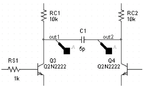
Analog example
In this section, basic techniques for performing waveform analysis are demonstrated using the analog circuit EXAMPLE.OPJ.
The example project EXAMPLE.OPJ is provided with your installed programs. When shipped, EXAMPLE.OPJ is set up with multiple analyses. For this example, the AC sweep, DC sweep, Monte Carlo/ worst-case, and small-signal transfer function analyses have been disabled. The specification for each of these disabled analyses remains intact. To run them from Capture in the future, from the PSpice menu, choose Edit Simulation Profile and enable the analyses.
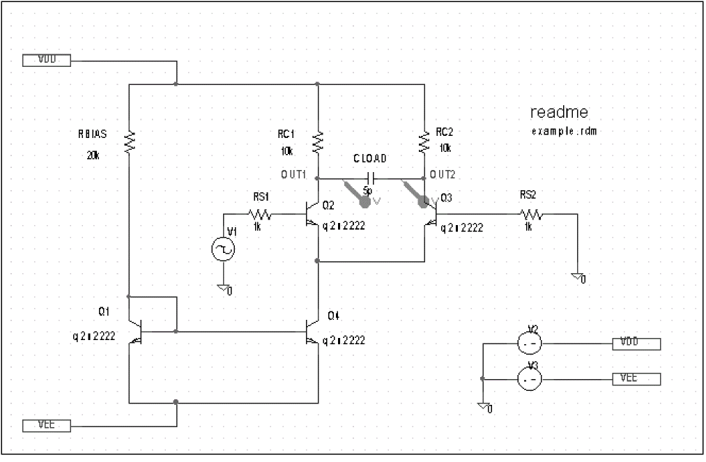
Figure 17-6 Example schematic EXAMPLE.OPJ
Running the simulation
The simulation is run with the Bias Point Detail, Temperature, and Transient analyses enabled. The temperature analysis is set to 35 degrees. The transient analysis is setup as follows:
Print Step 20ns Final Time 1000ns Enable Fourier selected Center Frequency 1Meg Output Vars V(OUT2)
To start the simulation
- From Capture’s File menu, point to Open and choose Project.
- Open the following project in your installation directory:
\TOOLS\PSPICE\CAPTURE_SAMPLES\ANASIM\ EXAMPLE\EXAMPLE.OPJ - From the PSpice menu, choose Run to start the simulation.
If PSpice A/D is set to show traces for all markers on startup, you will see the V(OUT1) and V(OUT2) traces when the Probe window displays. To clear these traces from the plot, from the Trace menu, choose Delete All Traces.
PSpice A/D generates a binary waveform data file containing the results of the simulation. A new Probe window appears with the waveform data file EXAMPLE.DAT already loaded (Figure 17-7).
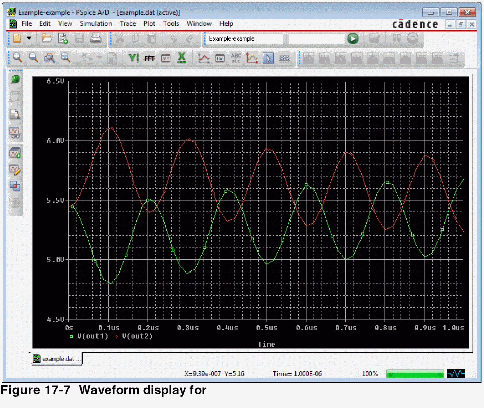
Because this sample project was set up as a transient analysis type, the data currently loaded are the results of the transient analysis.
Displaying voltages on nets
After selected an analysis, voltages on nets and currents into device pins can be displayed in the Probe windows using either schematic markers or output variables (as will be demonstrated in this example).
To display the voltages at the OUT1 and OUT2 nets using output variables
- From the Trace menu, choose Add Trace to display the Add Traces dialog box.
The Simulation Output Variables frame displays a list of valid output variables. - Click V(OUT1) and V(OUT2), then click OK. The Probe window should look similar to Figure 17-7.
Mixed analog/digital tutorial
In this tutorial, you will use PSpice A/D to simulate a simple, mixed analog/ digital circuit. You will then analyze the output by:
- simultaneously displaying analog and digital traces along a common time axis, and
- displaying digital data values and features unique to mixed analog/ digital circuit analysis, such as identification of digital nets inserted by PSpice A/D.
About digital states
All digital states are supported in PSpice A/D. Logic levels appear as shown below.
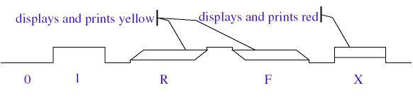
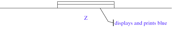
Nets with the Z strength (at any level) are displayed as a triple line as shown below.
About the oscillator circuit
The circuit you will simulate and analyze is a mixed analog/digital oscillator using Schmitt trigger inverters, an open-collector output inverter, a standard inverter, a JK flip-flop, a resistor, and a capacitor. The design is shown in Figure 17-8.
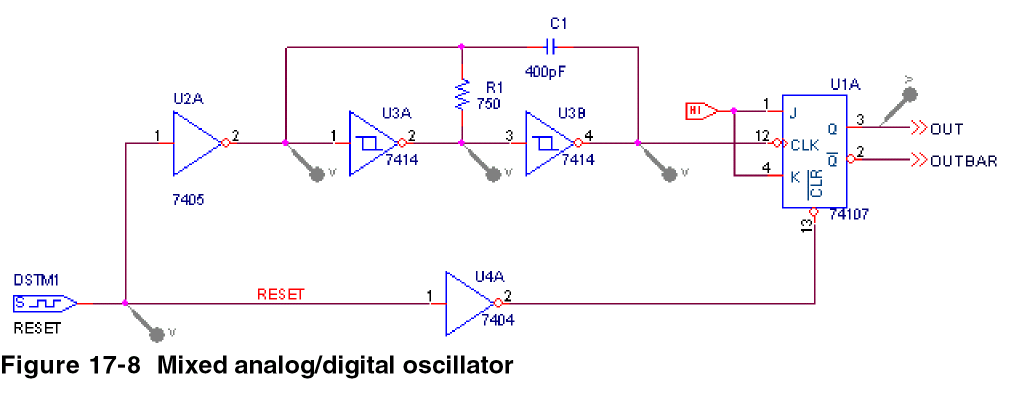
The circuit uses a one-bit digital stimulus device, DSTIM1. The device is connected to the rest of the circuit by a single pin and creates a reset pulse, which resets the flip-flop.
Setting up the design
Set up and simulate the oscillator circuit using Capture.
To open the design file
- From Capture’s File menu, point to Open and choose Project.
- Open the following project in your OrCAD X installation directory:
\TOOLS\PSPICE\CAPTURE_SAMPLES\MIXSIM\OSC\OSC.OPJ
To clear markers
- From Capture’s PSpice menu, point to Markers and choose Delete All.
Running the simulation
To run the simulation
- From Capture’s PSpice menu, choose Edit Simulation Profile and set the Run To Time to 5us.
- From Capture’s PSpice menu, choose Run.
Because the oscillator circuit used here has been run with only a transient analysis, PSpice A/D automatically selects the transient analysis data section from the waveform data file. This means that the Available Selection dialog box is skipped and a Probe window appears immediately.
Analyzing simulation results
To view the clock input to the inverter
- From PSpice A/D’s Trace menu, choose Add Trace to display the Add Traces dialog box.
- In the Simulation Output Variables list, click V(U3A:A) to plot the input voltage to the inverter.
- Click OK.
To add a second y-axis to avoid analog trace overlap
- From the Plot menu, choose Axis Settings to display the Axis Settings dialog box.
The X Axis tab is active by default.
You can also open the X Axis tab in the Axis Settings dialog box by double-clicking the x-axis in the Probe window.- In the Data Range frame, choose User Defined and set the range from 0us to 5us, if this is not already set.
- In the Scale frame, select Linear, if this is not already set.
- Click the Y Axis tab.
You can also open the Y Axis tab in the Axis Settings dialog box by double-clicking the y-axis in the Probe window.- In the Data Range frame, choose User Defined and set the range from -5 to 5. This will change the range for the current y-axis.
- Click OK.
In the Y Axis Settings dialog box, you can change the settings for another y-axis by selecting it from the Y Axis Number box.
- From the Plot menu, choose Add Y Axis.
The Probe window display should now look like Figure 17-9 below.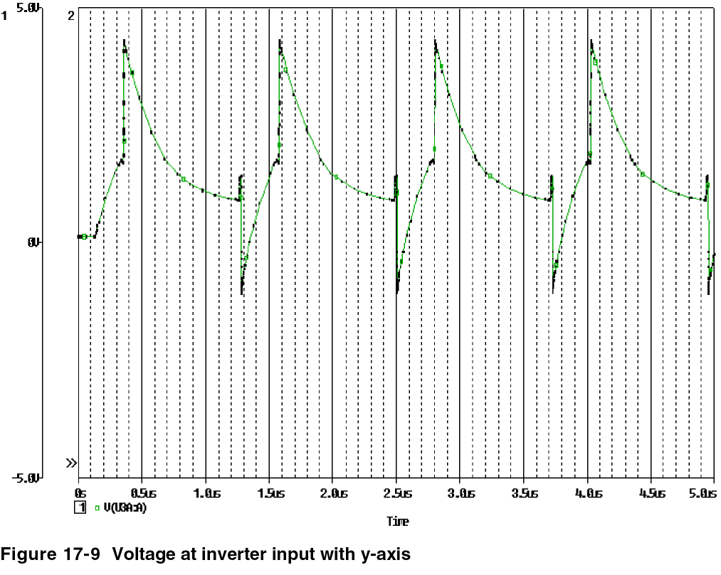
Note that the V(U3A:A) label at the bottom of the plot is preceded by a boxed 1. This indicates that the far-left y-axis applies to the V(U3A:A) waveform.
To view traces for V(CLK), RESET, and OUT
- From the Trace menu, choose Add Trace to display the Add Traces dialog box.
- In the Simulation Output Variables list, click V(U1A:CLK), RESET, and OUT.
The trace names appear in the Trace Expression text box.
You can add up to 75 digital traces to the digital portion of the plot. If you add more traces than can be displayed, PSpice A/D scrolls the traces upwards so you can see the last trace added. A + character in front of the highest or lowest trace name indicates that there are more traces above or below the marked traces. - Click OK to plot the traces.
The plot displays a digital area above the analog area as shown in Figure 17-10 below.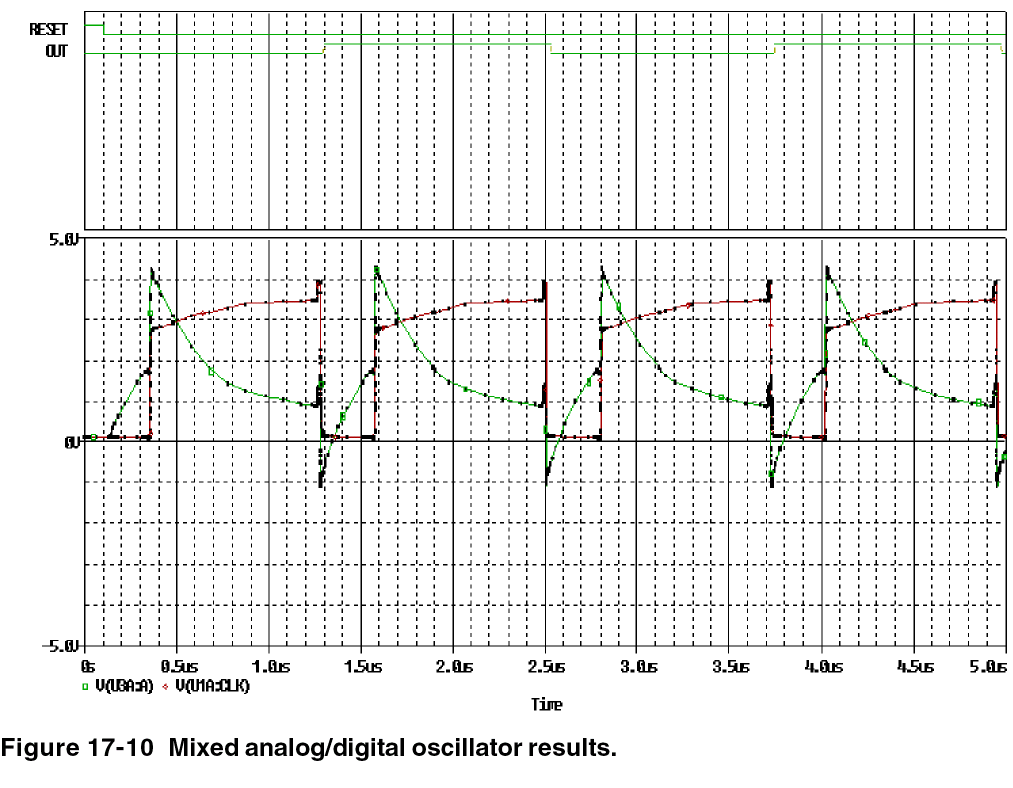
User interface features for waveform analysis
PSpice A/D provides direct manipulation techniques and shortcuts for analyzing waveform data. These techniques are described below.
Many of the menu commands in PSpice A/D have equivalent keyboard shortcuts. For instance, after placing a selection rectangle in the analog portion of the plot, you can type Ctrl+A instead of choosing Area from the View menu. For a list of shortcut keys, see PSpice A/D Help.
Zoom regions
PSpice A/D provides a direct manipulation method for marking the zoom region in either the digital or the analog area of the plot.
I or i to zoom in and o or O to zoom out in the Probe window.To zoom in or out
- Do one of the following on the toolbar:
- Click the View In toolbar button
 to zoom in by a factor of 2 around the point you specify.
 - Click the View Out toolbar button
 to zoom out by a factor of 2 around the point you specify.
- Click the View In toolbar button
To zoom in the digital area using the mouse
- In the digital area, drag the mouse pointer left or right to produce two vertical bars.
Click the mouse anywhere on the plot to remove the vertical bars without zooming.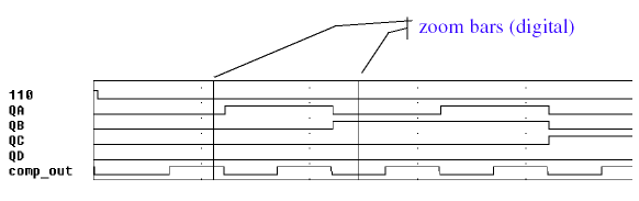
- From the View menu, point to Zoom, then choose Area.
PSpice A/D changes the plot display to the area in between the selection bars. If the plot includes an analog area, it is zoomed in as well.
To zoom in the analog area using the mouse
- Drag the mouse pointer to make a selection rectangle as shown below.
Click anywhere on the plot to remove the selection rectangle without zooming.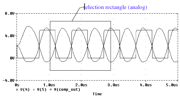
- From the View menu, point to Zoom, then choose Area.
PSpice A/D changes the plot to display the region within the selection rectangle. The digital portion of the display, if present, is also zoomed.
Scrolling traces
By default, when a plot is zoomed or when a digital plot contains more traces than can be displayed in the visible area, standard scroll bars appear to the right or at the bottom of the plot area as necessary. These can be used to pan through the data. You can configure scroll bars so they are always present or are never displayed.
To configure scroll bars
- In PSpice A/D, from the Tools menu, choose Options.
- In the Use Scroll Bars frame, choose one of the scroll bars options, as described below.
Choose this option... To do this... Auto
Have scroll bars appear when a plot is zoomed or when additional traces are displayed in the plot but are not visible (default).
Never
Never display scroll bars. This mode provides maximum plot size and is useful on VGA and other low resolution displays.
Always
Display scroll bars at all times. However, they are disabled if the corresponding axis is full scale.
Showing and hiding traces
You can show or hide one or more traces by right-clicking on a trace and choosing one of the following options:
- Hide Trace: Hides the selected trace.
- Hide All Traces: Hides all displayed traces.
- Show All Traces: Shows all traces.
You can also right-click on the probe window to choose either Show All Traces or Hide All Traces.
Sizing digital plots
Sizing bars can be used to change the digital plot size instead of choosing Digital Size from the Plot menu. The digital trace name sizing bar is at the left vertical boundary of the digital plot. If an analog plot area is displayed simultaneously with the digital plot, there is an additional plot sizing bar at the bottom horizontal boundary of the digital plot.
To set the digital plot size using the mouse
- Display at least one digital trace and one analog trace in the Probe window for which you want to set the digital size.
- To change the bottom position of the digital Probe window, do the following:
- Place the mouse pointer between the analog and digital parts of the plot.
- Click the plot separator.
- Drag the plot separator until you have the digital size you want.
- To change the left side of the digital Probe window, do the following:
- Place the mouse pointer at the left edge of the digital Probe window you want to resize.
- Click the left edge.
- Drag the left edge of the digital Probe window to adjust the space available for displaying digital trace names.
To set the digital plot size using menu options
- Display at least one digital trace in the plot for which you want to set the digital size.
- From the Plot menu, choose Digital Size.
- In the Digital Size dialog box, set the following:
- Percentage of Plot to be Digital
- Length of Digital Trace Name
- Click OK.
Modifying trace expressions and labels
You can modify trace expressions, text labels, and ellipse labels that are currently displayed within the Probe window, thus eliminating the need to delete and recreate any of these objects.
- To place a label, click Plot, point to Label and then choose the desired type of object you want to place.
You can click Font and specify a different font style for each label text.For information about adding labels (including text, line, poly-line, arrow, box, circle, ellipse, and mark), refer to PSpice A/D Help.
To modify trace expressions
- Click the trace name to select it (selection is indicated by a color change).
- From the Edit menu, choose Modify Object.
You can also double-click the trace name to modify the trace expression. - In the Modify Trace dialog box, edit the trace expression just as you would when adding a trace.
For more information on adding traces, see Adding traces from specific loaded waveform data files and To add traces using output variables.
To modify text and ellipse labels
- Click the text or ellipse to select it (selection is indicated by a color change).
- From the Edit menu, choose Modify Object.
You can also double-click a text or ellipse label to modify it. - Edit the label by doing one of the following:
- In the Ellipse Label dialog box, change the inclination angle.
- In the Text Label dialog box, change the text label.
To modify default label font
- Choose Tools - Options to open the Probe Settings dialog box
- Click the Font Settings tab.
- Click Change Label Font to open the Font dialog box.
- Specify the type, style, size, color, and effects.
- Click OK.
You must restart PSpice A/D for the font changes.
Moving and copying trace names and expressions
Trace names and expressions can be selected and moved or copied, either within the same Probe window or to another Probe window.
To copy or move trace names and expressions
- Click one or more (Shift+click) trace names. Selected trace names are highlighted.
- From the Edit menu, choose Copy or Cut to save the trace names and expressions to the clipboard. Cut removes trace names and traces from the Probe window.
- In the Probe window where traces are to be added, do one of the following:
- To add trace names to the end of the currently displayed set, choose Paste from the Edit menu.
- To add traces before a currently displayed trace name, select the trace name and then choose Paste from the Edit menu.
- Click OK.
When adding a trace to a Probe window, you can make the trace display name different from the trace expression:- From the Trace menu, choose Add Trace.
- In the Trace Expression text box, enter a trace expression using the syntax:
trace_expression[;display_name]
Here are some considerations when copying or moving trace names and expressions into a different Probe window:
- If the new Probe window is reading the same waveform data file, the copied or moved trace names and expressions display traces that are identical to the original selection set.
- If the new Probe window is reading a different waveform data file, the copied or moved names and expressions display different traces generated from the new data.
For example, suppose two waveform data files,MYSIM.DATandYOURSIM.DATeach contain a V(2) waveform. Suppose also that two Probe windows are currently displayed where window A is loaded withMYSIM.DAT, and window B is loaded withYOURSIM.DAT.
When V(2) is copied from window A to window B, the trace looks different because it is determined by data fromYOURSIM.DATinstead ofMYSIM.DAT.
Copying and moving labels
Labels can be selected and moved or copied, either within the same Probe window or to another Probe window.
For information about adding labels (including text, line, poly-line, arrow, box, circle, ellipse, and mark), refer to PSpice Help.
To copy labels
- Select one or more (Shift+click) labels, or select multiple labels by drawing a selection rectangle. Selected labels are highlighted.
- From the Edit menu, choose Copy or Cut to save the labels to the clipboard.
Cut removes labels from the Probe window. - Switch to the Probe window where labels are to be added, and from the Edit menu, choose Paste.
- Click on the new location to place the labels.
To move labels
- Select one or more (Shift+click) labels, or select multiple labels by drawing a selection rectangle. Selected labels are highlighted.
- Move the labels by dragging them to a new location.
Tabulating trace data values
You can generate a table of data points reflecting one or more traces in the Probe window and use this information in a document or spreadsheet.
To view the trace data values table
- Select one or more (Shift+click) trace names. Selected trace names are highlighted.
- From the Edit menu, choose Copy or Cut to save the trace data point values to the Clipboard.
Cut removes traces from the Probe window. - In Clipboard Viewer, from the Display menu, choose either Text or OEM Text.
To export the data points to other applications
- Select one or more (Shift+click) trace names. Selected trace names are highlighted.
- From the Edit menu, choose Copy or Cut to save the trace data point values to the Clipboard.
Cut removes traces from the Probe window. - Paste the data from the Clipboard into a text editor, a spreadsheet program, or a technical computing program (such as Mathcad).
- Save the file.
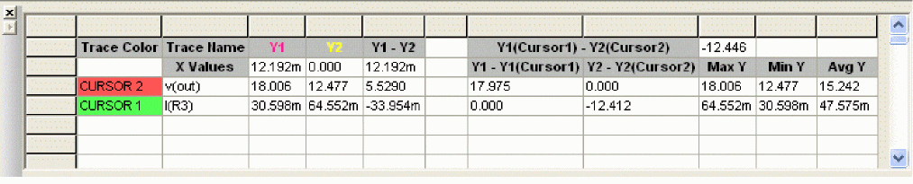
Using cursors
When one or more traces are displayed, you can use cursors to display the exact coordinates of two points on the same trace, or points on two different traces. In addition, differences are shown between the corresponding coordinate values for the two cursors.
The cursor information is shown in a dockable cursor window. The cursor window displays the trace name, trace color, and the different Y-axis values, including differences on the Y-axis of cursor values.
Displaying cursors
To display both cursors
- Choose Trace – Cursor – Display.
The dockable cursor window appears, showing the current position of the cursor on the x-axis and y-axis. As you move the cursors, the values in this window change.
In the analog area of the plot (if any), both cursors are initially placed on the trace listed first in the trace legend. The corresponding trace symbol is outlined with a dashed line.
In the digital area of the plot (if any), both cursors are initially placed on the trace named first along the y-axis. The corresponding trace name is outlined with a dashed line.
Moving cursors
To move cursors along a trace using menu commands
- Choose Trace – Cursor.
- Next, choose Peak, Trough, Slope, Min, Max, Point, or Search Commands.
For more information about the cursor commands, see PSpice A/D Help.
To move cursors along a trace using the mouse
- Use the right and left mouse buttons as described in Table 17-8 below.
Table 17-8 Mouse actions for cursor control
Click this... To do this with the cursors... cursor assignment Left-click the analog trace symbol or digital trace name.
Associate the first cursor with the selected trace.
Right-click the analog trace symbol or digital trace name.
Associate the second cursor with the selected trace.
cursor movement Left-click in the display area.
Move the first cursor to the closest trace segment at the X position.
Right-click in the display area.
Move the second cursor to the closest trace segment at the X position.
To move cursors along a trace using the keyboard
- Use key combinations as described in Table 17-9.
Table 17-9 Key combinations for cursor control
Us this key combination... To do this with the cursors... Ctrl+Left arrow key and Ctrl+Right arrow key
Change the trace associated with the first cursor.
Shift+Ctrl+Left arrow key and Shift+Ctrl+Right arrow key
Change the trace associated with the second cursor.
Left arrow key and Right arrow key
Move the first cursor along the trace.
Shift+Left arrow key and Shift+Right arrow key
Move the second cursor along the trace.
Home
Move the first cursor to the beginning of the trace.
Shift+Home
Move the second cursor to the beginning of the trace.
End
Move the first cursor to the end of the trace.
Shift+End
Move the second cursor to the end of the trace.
Applying cursors to a different trace
If you want to apply the cursors to a different trace, click the trace symbol in the plot legend for the trace you want to change to.
To freeze the cursor, do one of the following:
- Choose Trace – Cursor – Freeze to freeze the cursor locations on the current trace.
OR
- Choose Tools – Options.
The Probe Settings dialog box opens. - Select the Cursor Settings tab.
- Select Show non-dockable(old) cursor window.
The Probe Cursor window appears. - Click the Probe Cursor window (below the title bar) to freeze the cursor locations on the current trace.
For more information about the cursor commands, see PSpice A/D Help.
Changing cursor properties
- Choose Tools – Options.
The Probe Settings dialog box opens. - Specify the width and color for the cursors in the Cursor Settings tab.
The cursor color is affected by the background color of the PSpice A/D probe window. As a result, you might see the cursors with a different color in the probe window. However, the colors are updated in the Cursor Settings tab also. Close the Probe Settings dialog box and open it again to view the changed color.
Dumping and copying cursor information
To dump cursor:
- Open the dockable cursor window.
- Right-click in this window and choose Dump to CSV File. The CSV file is created at the location of the
.datfile.
To open the CSV file location, choose File – Open File Location. The CSV file can be opened using tools such as Microsoft Excel.
To copy cursor values:
- Select the cursor values that you want to copy in the dockable cursor window.
- Right-click and choose Copy.
- Open any text editor and paste the content from clipboard.
Example: Using cursors from non-dockable (old) cursor window
Following figure shows both cursors positioned on the Out signal in the digital area of a plot, and both cursors on the V(1) waveform in the analog area of the plot.
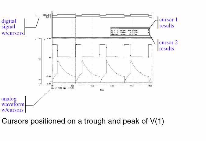
Cursor 1 is positioned on the first trough (dip) of the V(1) waveform. Cursor 2 is positioned on the second peak of the same waveform.
In the Probe Cursor window, cursor 1 and cursor 2 coordinates are displayed (A1 and A2, respectively) with their difference shown in the bottom line (dif). The logic state of the Out signal is also displayed to the right of the cursor coordinates.
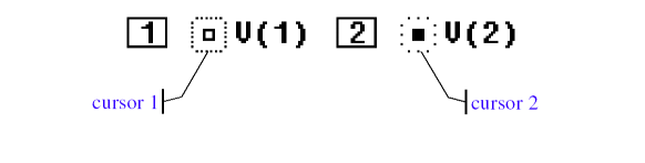
The mouse buttons are also used to associate each cursor with a different trace by clicking appropriately on either the analog trace symbol in the legend or on the digital trace name (see Table 17-8). These are outlined in the pattern corresponding to the associated cursor’s crosshair pattern. In the above example, right-clicking the V(2) symbol will associate cursor 2 with the V(2) waveform. The analog legend now appears as shown below.
The Probe Cursor window also updates the A2 coordinates to reflect the X and Y values corresponding to the V(2) waveform.
For more information about cursors, see PSpice A/D Help.
Tracking digital simulation messages
PSpice A/D provides explanatory messages for errors that occur during a digital simulation with their corresponding waveforms. You can view messages from:
- the Simulation Message Summary dialog box, or
- the waveform display.
Message tracking from the message summary
A message summary is available for simulations where diagnostics have been logged to the waveform data file. You can display the message summary:
- When loading a waveform data file (click OK when the Simulation Errors dialog box appears).
- Anytime by choosing Simulation Messages from the View menu.
The Simulation Message Summary dialog box
The Simulation Message Summary dialog box lists message header information.
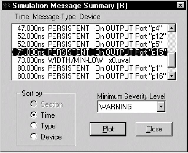
You can filter the messages displayed in the list by selecting a severity level from the Minimum Severity Level drop-down menu. Messages are categorized (in decreasing order of severity) as FATAL, SERIOUS, WARNING, or INFO (informational).
When you select a severity level, the Message Summary displays only those messages with the chosen severity or higher. By default, the minimum severity level displayed is SERIOUS.
Example: If you select WARNING as the minimum severity level, the Simulation Message Summary dialog box will display WARNING, SERIOUS, and FATAL messages.
To display waveforms associated with messages
- In the Simulation Message Summary dialog box, double-click a message.
For most message conditions, a Probe window appears that contains the waveforms associated with the simulation condition, along with detailed message text.
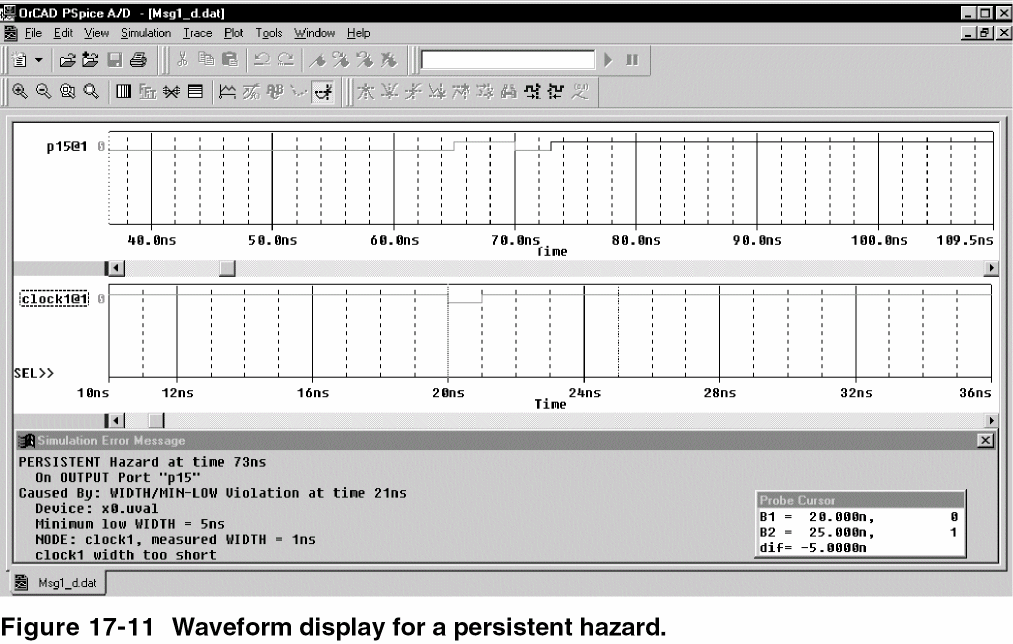
Persistent hazards
If a PERSISTENT HAZARD message is displayed, two plots appear (see Figure 17-11), containing the following:
- the waveforms that initially caused the timing violation or hazard (lower plot)
- the primary outputs or internal state devices to which the condition has propagated (upper plot)
Message tracking from the waveform
Trace segments with associated diagnostics are displayed in the foreground color specified in your PSpice.ini file. This color is different from those used for standard state transitions.
To display explanatory message text
- Double-click within the tagged region of a trace.
Trace expressions
Traces are referred to by output variable names. Output variables are similar to the PSpice output variables specified in the Simulation Settings dialog box for noise, Monte Carlo, worst-case, transfer function, and Fourier analyses. However, there are additional alias forms that are valid for trace expressions. Both forms are discussed here.
To add traces using output variables
- From the Trace menu, choose Add Trace to display the Add Traces dialog box.
- Construct a trace expression using any combination of these controls:
- In the Simulation Output Variables frame, click output variables.
You can display a subset of the available simulation output variables by selecting or clearing the variable type check boxes in the Simulation Output Variables frame. Variable types not generated by the circuit simulation are dimmed. - In the Functions or Macros frame, select operators, functions, constants, or macros.
- In the Trace Expression text box, type in or edit output variables, operators, functions, constants, or macros.
For more information about trace expressions, see Analog trace expressions and Digital trace expressions.
- In the Simulation Output Variables frame, click output variables.
- If you want to change the name of the trace expression as it displays in the Probe window, use the following syntax:
trace expression;display name - Click OK.
Basic output variable form
This form is representative of those used for specifying some PSpice A/D analyses.
<output>[AC suffix](<name>[,name])
| This placeholder... | Means this... |
|---|---|
|
<output> |
type of output quantity: V for voltage or I for current (digital values do not require a prefix) |
|
[AC suffix]* |
quantity to be reported for an AC analysis. For a list of valid AC suffixes, see Table 17-14 |
|
<name>[,name] |
specifies either the net or (+ net, - net) pair for which the voltage is to be reported, or the device for which a current is reported, where:
A fully qualified device name consists of the full hierarchical path followed by the device’s reference designator. |
Output variable form for device terminals
This form can only be specified for trace expressions. The primary difference between this and the basic form is that the terminal symbol appears before the net or device name specification (whereas the basic form treats this as the pin name within the pin id).
<output>[terminal]*[AC suffix](<name>[,name])
| This placeholder... | Means this... |
|---|---|
|
<output> |
type of output quantity: V for voltage, I for current, or N for noise (digital values do not require a prefix) |
|
[terminal]* |
one or more terminals for devices with more than two terminals; for a list of terminal IDs, see Table 17-16 |
|
[AC suffix]* |
quantity to be reported for an AC analysis; for a list of valid AC suffixes, see Table 17-14 |
|
<name>[,<name>]) |
net, net pair, or fully qualified device name; for a list of device types, see Table 17-15 and Table 17-16 |
Table 17-12 summarizes the valid output formats. Table 17-13 provides examples of equivalent output variables. Note that some of the output variable formats are unique to trace expressions.
| Format | Meaning |
|---|---|
| Voltage variables | |
|
V[ac](< +analog net > [,< -analog net >]) |
Voltage between + and - analog net ids |
|
V<pin name>[ac](< device >) |
Voltage at pin name of a device |
|
V< x >[ac](< 3 or 4-terminal device >) |
Voltage at non-grounded terminal x of a 3 or 4-terminal device |
|
V< z >[ac](< transmission line device >) |
Voltage at end z of a transmission line device (z is either A or B) |
| Current variables | |
|
I[ac](< device >) |
Current into a device |
|
I< x >[ac](< 3 or 4-terminal device >) |
Current into terminal x of a 3 or 4-terminal device |
|
I< z >[ac](< transmission line device >) |
Current into end z of a transmission line device (z is either A or B) |
| Digital signal and bus variables | |
|
< digital net >[;< display name >] |
Digital state at digital net labeled as display name |
|
{< digital net >*}[;< display name >] [;< radix >] |
Digital bus labeled as display name and of specified radix |
| Sweep variables | |
|
< DC sweep variable > |
name of any variable used in the DC sweep analysis |
|
FREQUENCY |
AC analysis sweep variable |
|
TIME |
transient analysis sweep variable |
| Noise variables | |
|
V[db](ONOISE) |
total RMS-summed noise at output net |
|
V[db](INOISE) |
total equivalent noise at input source |
|
NTOT(ONOISE) |
sum of all noise contributors in the circuit |
|
N< noise type >(< device name >) |
contribution from noise type of device name to the total output noise3 |
| A basic form | An alias equivalent | Meaning |
|---|---|---|
|
V(NET3,NET2) |
(same) |
voltage between analog nets labeled NET3 and NET2 |
|
V(C1:1) |
V1(C1) |
voltage at pin1 of capacitor C1 |
|
VP(Q2:B) |
VBP(Q2) |
phase of voltage at base of bipolar transistor Q2 |
|
V(T32:A) |
VA(T32) |
voltage at port A of transmission line T32 |
|
I(M1:D) |
ID(M1) |
current through drain of MOSFET device M1 |
|
QA |
(same) |
digital state at net QA |
|
{IN1, IN2, IN3}; |
(same) |
digital bus made of 3 digital nets (IN1, IN2, IN3) named MYBUS displayed in hexadecimal |
|
VIN |
(same) |
voltage source named VIN |
|
FREQUENCY |
(same) |
AC analysis sweep variable |
|
NFID(M1) |
(same) |
flicker noise from MOSFET M1 |
| Suffix | Meaning of output variables |
|---|---|
|
none |
magnitude |
|
DB |
magnitude in decibels |
|
G |
group delay (-dPHASE/dFREQUENCY) |
|
I |
imaginary part |
|
M |
magnitude |
|
P |
phase in degrees |
|
R |
real part |
| Two-terminal device type | Device type letter |
|---|---|
|
capacitor |
C |
|
diode |
D |
|
voltage-controlled voltage source |
E |
|
current-controlled current source2 |
F |
|
voltage-controlled current source2 |
G |
|
current-controlled voltage source2 |
H |
|
independent current source |
I |
|
inductor |
L |
|
resistor |
R |
|
voltage-controlled switch2 |
S |
|
independent voltage source |
V |
|
current-controlled switch2 |
W |
| Three & four-terminal device type | Device type letter | Terminal IDs |
|---|---|---|
|
GaAs MOSFET |
B |
D (drain) G (gate) S (source) |
|
Junction FET |
J |
D (drain) G (gate) S (source) |
|
MOSFET |
M |
D (drain) G (gate) S (source) B (bulk, substrate) |
|
Bipolar transistor |
Q |
C (collector) B (base) E (emitter) S (substrate) |
|
transmission line |
T |
A (near side) B (far side) |
|
IGBT |
Z |
C (collector) G (gate) E (emitter) |
| Device type | Noise types | Meaning |
|
B (GaAsFET) |
FID |
flicker noise |
|
D (diode) |
FID |
flicker noise |
|
Digital Input |
RHI |
thermal noise associated with RHI |
|
Digital Output |
TOT |
total noise |
|
J (JFET) |
FID |
flicker noise |
|
M (MOSFET) |
FID |
flicker noise |
|
Q (BJT) |
FIB |
flicker noise |
|
R (resistor) |
TOT |
total noise |
|
Iswitch |
TOT |
total noise |
|
Vswitch |
TOT |
total noise |
Analog trace expressions
Trace expression aliases
Analog trace expressions vary from the output variables used in simulation analyses because analog net values can be specified by:
<output variable>[;display name]
as opposed to the <output variable> format used in analyses. With this format, the analog trace expression can be displayed in the analog legend with an optional alias.
Arithmetic functions
Arithmetic expressions of analog output variables use the same operators as those used in simulation analyses (by means of part property definitions in Capture). You can also include intrinsic functions in expressions. The intrinsic functions available for trace expressions are similar to those available for PSpice math expressions, but with some differences, as shown in Table 17-18. A complete list of PSpice arithmetic functions can be found in Table 3-4.
| Probe function | Description | Available in PSpice A/D? |
|---|---|---|
|
ABS(x) |
|x| |
YES |
|
SGN(x) |
+1 (if x>0), 0 (if x=0), -1 (if x<0) |
YES |
|
SQRT(x) |
x1/2 |
YES |
|
EXP(x) |
e x |
YES |
|
LOG(x) |
ln(x) |
YES |
|
LOG10(x) |
log(x) |
YES |
|
M(x) |
magnitude of x |
YES |
|
P(x) |
phase of x (degrees) |
YES |
|
R(x) |
real part of x |
YES |
|
IMG(x) |
imaginary part of x |
YES |
|
G(x) |
group delay of x (seconds) |
NO |
|
PWR(x,y) |
|x|y |
YES |
|
SIN(x) |
sin(x) |
YES |
|
COS(x) |
cos(x) |
YES |
|
TAN(x) |
tan(x) |
YES |
|
ATAN(x) |
tan -1 (x) |
YES |
|
d(x) |
derivative of x with respect to the x-axis variable |
YES |
|
s(x) |
integral of x over the range of the x-axis variable |
YES |
|
AVG(x) |
running average of x over the range of the x-axis variable |
NO |
|
AVGX(x,d) |
running average of x from X_axis_value(x)-d to X_axis_value(x) |
NO |
|
RMS(x) |
running RMS average of x over the range of the x-axis variable |
NO |
|
DB(x) |
magnitude in decibels of x |
NO |
|
MIN(x) |
minimum of the real part of x |
NO |
|
MAX(x) |
maximum of the real part of x |
NO |
|
ENVMIN(x,d) |
Envelope of x.Valley lows selected have a minimum number of d consecutive datapoints. |
NO |
|
ENVMAX(x,d) |
Envelope of x. Peaks selected have a minimum number of d consecutive datapoints. |
NO |
Rules for numeric values suffixes
Explicit numeric values are entered in trace expressions in the same form as in simulation analyses (by means of part properties in Capture), with the following exceptions:
- Suffixes M and MEG are replaced with m (milli, 1E-3) and M (mega, 1E+6), respectively.
- MIL and mil are not supported.
- With the exception of the m and M scale suffixes, PSpice A/D is not case sensitive; therefore, upper and lower case characters are equivalent.
Example: V(5) and v(5) are equivalent in trace expressions.
Unit suffixes are only used to label the axis; they never affect the numerical results. Therefore, it is always safe to leave off a unit suffix.
Example: The quantities 2e-3, 2mV, and .002v all have the same numerical value. For axis labeling purposes, PSpice A/D recognizes that the second and third forms are in volts, whereas the first is dimensionless.
PSpice A/D also knows that W=V·A, V=W/A, and A=W/V. So, if you add this trace:
V(5)*ID(M13)
the axis values are labeled with W.
For a demonstration of analog trace presentation, see Analog example
The units to use for trace expressions are shown in Table 17-19.
| Symbol | Unit |
|---|---|
|
V |
volt |
|
A |
amps |
|
W |
watt |
|
d |
degree (of phase) |
|
s |
second |
|
Hz |
hertz |
Digital trace expressions
Digital output variables in trace expressions vary from those used in simulation analyses as follows:
- Digital net values are specified by:
<digital net>[;display name]
as opposed to the <digital net> format used for analyses. With this format, the digital signal can be displayed on the digital plot with an optional alias. - The output from several digital nets can be collected into a single output of higher radix known as a bus.
Example: You can request that four bus lines be displayed together as one hexadecimal digit. You can combine up to 32 digital signals into a bus.
A bus is formed by enclosing a list of digital net names (separated by blanks or commas) within braces according to the format:
{<high-order net> [mid-order net]* <low-order net>}
The elements of the bus definition, taken left to right, specify the output values of the bus from high order to low order.
Example: { Q2, Q1, Q0 } specifies a 3-bit bus whose high-order bit is the digital value at net Q2.
By definition, a digital signal is any digital net value or a logical expression involving digital nets. For the digital output variable formats described earlier, you can use a digital signal expression everywhere a net name is expected. You can also form buses into expressions using both logical and arithmetic operators.
As a result, the generalized form for defining a digital trace is:
<digital trace expression> [;display name [;radix]]
Exception: You can display your radix designation option with the digital trace expression by leaving the display name blank and using the following syntax:
digital trace expression;;radix
| This placeholder... | Means this... |
|---|---|
|
digital trace expression |
expression of digital buses or digital signals. |
|
display name |
name that will be displayed on the screen; if no display name is specified, the actual trace expression is used; if a display name is given, it is available for use in subsequent trace definitions. |
|
radix |
applies only to bus expressions and denotes the radix in which the bus value is to be displayed; the radix is specified as: H or X hexadecimal (default) |
Table 17-21 presents the operators available for digital signal and bus expressions listed in order of precedence (high to low).
| Operator | Meaning |
|---|---|
|
() |
grouping |
|
~ |
logical complement |
|
* |
multiplication (bus values only) |
|
/ |
division (bus values only) |
|
+ |
addition (bus values only) |
|
- |
subtraction (bus values only) |
|
& |
and |
|
^ |
exclusive or |
|
| |
or |
An arithmetic or logical operation between two bus operands results in a bus value that is as wide as is necessary to contain the result. Prior to the operation, if necessary, the shorter operand is extended to the width of the longer operand by zero-filling on the high-order end.
An arithmetic or logical operation between a bus operand and a signal operand results in a bus value. Prior to the operation, the signal is converted to a bus of width one, then extended if necessary.
You can use signal constants in signal expressions. Specify them as shown in Table 17-22.
| Signal Constant | Meaning |
|---|---|
|
’0 |
low |
|
’1 |
high |
|
’F |
falling |
|
’R |
rising |
|
’X |
unknown |
|
’Z |
high impedance |
You can use bus constants in bus expressions. Specify them as strings of the form:
r'ddd
| This placeholder... | Means this... |
|---|---|
|
r |
case-insensitive radix specifier (x, h, d, o, or b) |
|
ddd |
string of digits appropriate to the specified radix |
| This notation... | Has this radix... |
|---|---|
|
x'3FFFF |
hexadecimal |
|
h'5a |
hexadecimal |
|
d'79 |
decimal |
|
o'177400 |
octal |
|
b'100110 |
binary |
For a discussion and demonstration of digital trace presentation, complete the Mixed analog/digital tutorial.
- Depending on the license available, you will access either PSpice A/D or PSpice Simulator.
You can use these markers instead of the built-in functions provided in output variable expressions (see Table 17-18). However, these markers are only available after defining a simulation profile for an AC Sweep/Noise analysis.
See Table 17-17 for a complete list of noise types by device type.
The pin name for two-terminal devices is either 1 or 2.
The controlling inputs for these devices are not considered terminals.
These variables report the contribution of the specified device’s noise to the total output noise in units of V2/Hz. This means that the sum of all device noise contributions is equal to the total output noise in V2/Hz, NTOT(ONOISE).
In PSpice A/D, this function is called DDT(x).
In PSpice A/D, this function is called SDT(x).
View the next document: 18 - Measurement Expressions
If you have any questions or comments about the OrCAD X platform, click on the link below.
Contact Us