09 - DC Sweep Analyses
DC Sweep
Minimum requirements to run a DC sweep analysis
Minimum circuit design requirements
| Swept variable type | Requirement |
|---|---|
|
voltage source |
voltage source with a DC specification (VDC, for example) |
|
temperature |
none |
|
current source |
current source with a DC specification (IDC, for example) |
|
model parameter |
PSpice A/D model (.MODEL) |
|
global parameter |
global parameter defined with a parameter block (.PARAM) |
Minimum program setup requirements
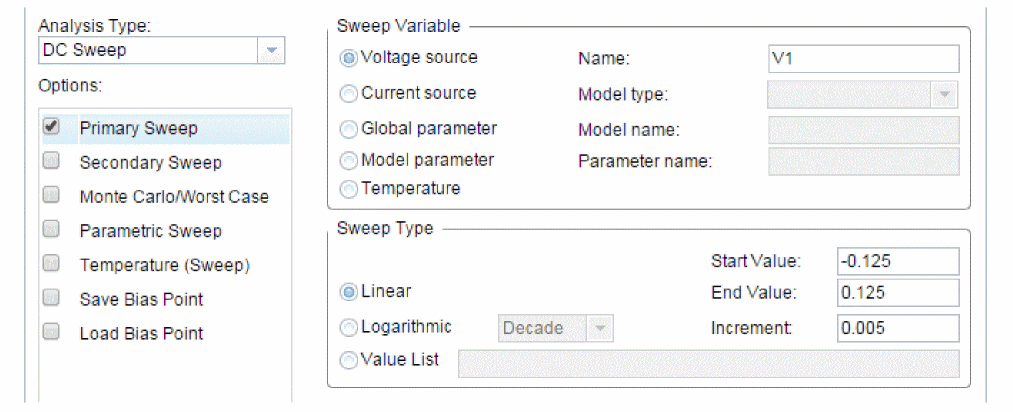
- In the design entry tool1, select New Simulation Profile or Edit Simulation Profile from the PSpice menu. (If this is a new simulation, enter the name of the profile and click OK.)
The Simulation Settings dialog box appears. - Under Analysis Type, select
DC Sweep. - For the Primary Sweep option, enter the necessary parameter values and select the appropriate check boxes to complete the analysis specifications.
- Click OK to save the simulation profile.
- Select Run under the PSpice menu to start the simulation.
Overview of DC sweep
The DC sweep analysis causes a DC sweep to be performed on the circuit. DC sweep allows you to sweep a source (voltage or current), a global parameter, a model parameter, or the temperature through a range of values. The bias point of the circuit is calculated for each value of the sweep. This is useful for finding the transfer function of an amplifier, the high and low thresholds of a logic gate, and so on.
For the DC sweep analysis specified in Figure 9-1, the voltage source V1 is swept from -0.125 volts to 0.125 volts by steps of 0.005. This means that the output has
(0.125 + 0.125)/0.005 +1 = 51 steps or simulation points.
A source with a DC specification (such as VDC or IDC) must be used if the swept variable is to be a voltage type or current source. To set the DC value, select Properties from the Edit menu, then click on the cell under the DC column and type in its value.
The default DC value of V1 is overridden during the DC sweep analysis and is made to be the swept value. All of the other sources retain their values.
After running the analysis, the simulation output file (EXAMPLE.OUT for the EXAMPLE.OPJ circuit in Figure 9-1) contains a table of voltages relating V1, node OUT1, and node OUT2.
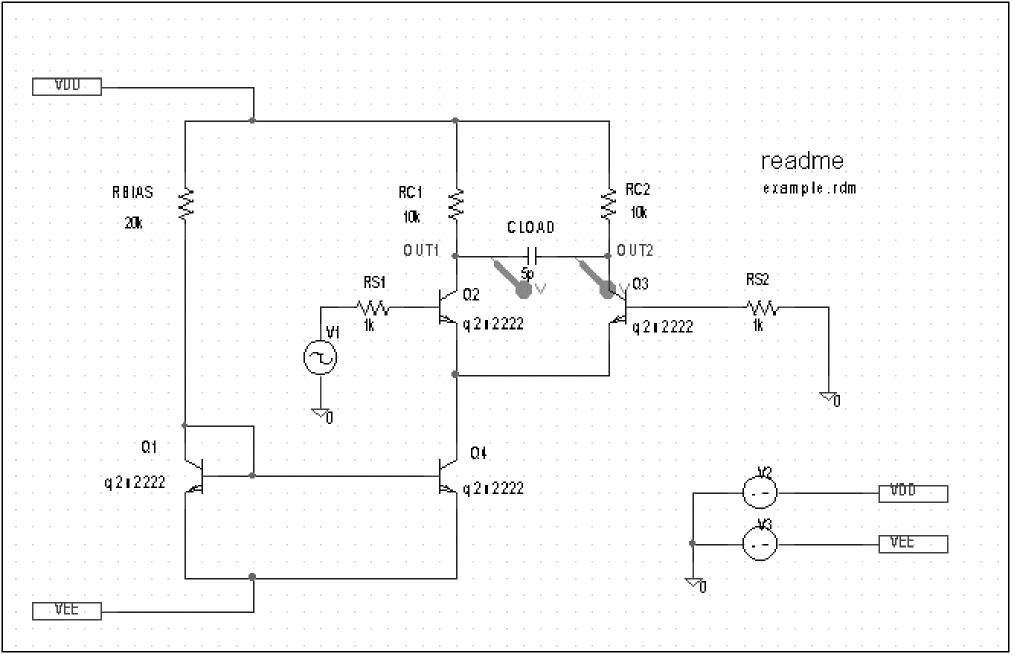
Figure 9-1 Example schematic EXAMPLE.OPJ.
To calculate the DC response of an analog circuit, PSpice A/D removes time from the circuit. This is done by treating all capacitors as open circuits, all inductors as shorts, and using only the DC values of voltage and current sources. A similar approach is used for digital devices: all propagation delays are set to zero, and all stimulus generators are set to their time-zero values.
In order to solve the circuit equations, PSpice A/D uses an iterative algorithm. For analog devices, the equations are continuous, and for digital devices, the equations are Boolean. If PSpice A/D cannot get a self-consistent result after a certain number of iterations, the analog/ digital devices are forced to the X value, and more iterations are done. Since X as input to a digital component gives X as output, the Boolean equations can always be solved this way.
If a digital node cannot be driven by known values during the DC iterations (for instance, the output of a flip-flop with the clock line held low), then its DC state will be X. Depending on the circuit, some, none, or all of the digital nodes may have the state X when the bias point is calculated.
Setting up a DC stimulus
To run a DC sweep or small-signal DC transfer analysis, you need to place and connect one or more independent sources and then set the DC voltage or current level for each source.
To set up a DC stimulus
- Place and connect one of these symbols in your schematic:
For voltage input Use this... When you are running... VDC
A DC Sweep and/or Bias Point (transfer function) analysis only.
VSRC
Multiple analysis types including DC Sweep and/or Bias Point (transfer function).
For current input Use this... When you are running... IDC
A DC Sweep and/or Bias Point (transfer function) analysis only.
ISRC
Multiple analysis types including DC Sweep and/or Bias Point (transfer function).
- Double-click the symbol instance to display the Parts spreadsheet appears.
- Click in the cell under the DC column to edit its value.
- Define the DC specification as follows:
Set this attribute... To this value... DC
DC_level
where DC_level is in volts or amps (units are optional). - Click OK twice to exit the dialog boxes.
Nested DC sweeps
A second sweep variable can be selected after a primary sweep value has been specified in the DC Sweep dialog box. When you specify a secondary sweep variable, it forms the outer loop for the analysis. That is, for every increment of the second sweep variable, the first sweep variable is stepped through its entire range of values.
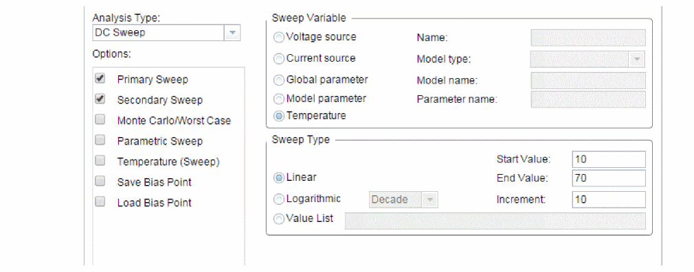
To set up a nested sweep
- Under Options, select the Secondary Sweep box for the DC Sweep Analysis type.
- Enter the necessary parameter values and select the appropriate check boxes to complete the analysis specifications.
Curve families for DC sweeps
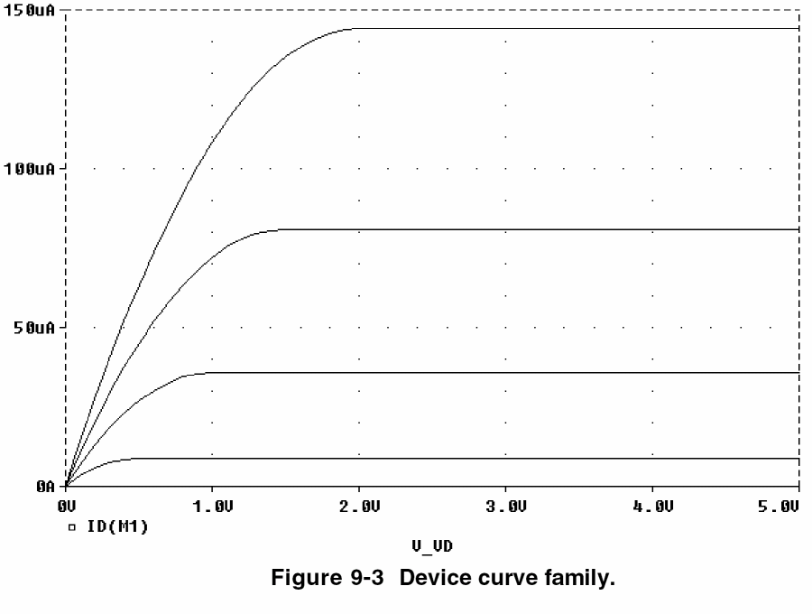
When a nested DC sweep is performed, the entire curve family is displayed. That is, the nested DC sweep is treated as a single data section (or you can think of it as a single PSpice A/D run).
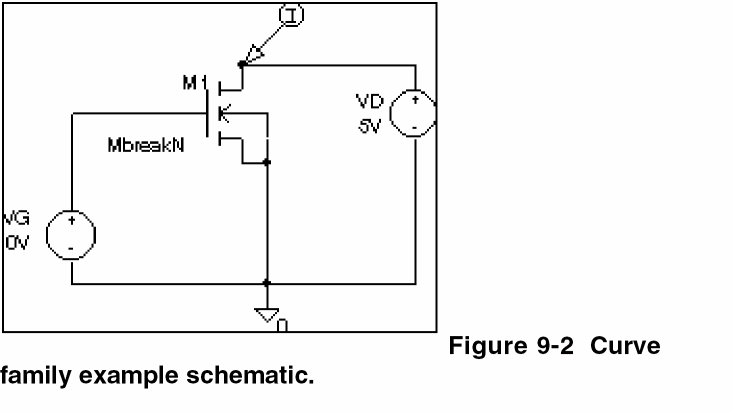
For the circuit shown in Figure 9-2, you can set up a DC sweep analysis with an outer sweep of the voltage source VG and an inner sweep of the voltage source VD as listed in Table 9-1.
| Primary sweep | Secondary sweep | |
|---|---|---|
|
Swept Var Type |
voltage source |
voltage source |
|
Sweep Type |
linear |
linear |
|
Name |
VD |
VG |
|
Start Value |
0 |
0 |
|
End Value |
5 |
2 |
|
Increment |
0.1 |
0.5 |
When the DC sweep analysis is run, add a current marker at the drain pin of M1 and display the simulation results in PSpice A/D. The result will look like Figure 9-3.
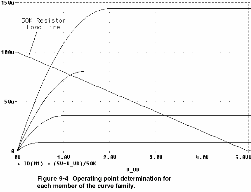
To add a load line for a resistor, add a trace that computes the load line from the sweep voltage. Assume that the X axis variable is the sweep voltage V_VD, which runs from 0 to 5 volts. The expression which will add a trace that is the load line for a 50 kohm resistor is:
(5V-V_VD)/50K
This can be useful for determining the bias point for each member of a curve family as shown in Figure 9-4.
Bias point
Minimum requirements to run a bias point analysis
Minimum circuit design requirements
None.
Minimum program setup requirements
- Under Analysis type in the Simulation Settings dialog box, select Bias Point.
- For the General Settings option, enter the necessary parameter values and select the appropriate check boxes to complete the analysis specifications.
- Click OK to save the simulation profile.
- In Capture, from the PSpice menu, select Run to start the simulation.
Overview of bias point
The bias point is calculated for any analysis whether or not the Bias Point analysis is enabled in the Simulation Settings dialog box. However, additional information is reported when the Bias Point analysis is enabled.
When Bias Point analysis is not enabled, only analog node voltages and digital node states are reported to the output file.
When the Bias Point analysis is enabled, the following information is reported to the output file:
- a list of all analog node voltages
- a list of all digital node states
- the currents of all voltage sources and their total power
- a list of the small-signal parameters for all devices
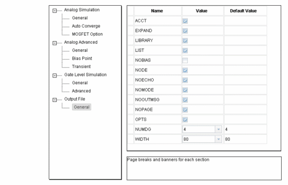
If Bias Point is enabled, you can suppress the reporting of the bias point analog and digital node values, as follows:
- Under the Options tab in the Simulation Settings dialog box, select Output file in the Category box.
- Uncheck the box for Bias point node voltages (NOBIAS).
Small-signal DC transfer
Minimum requirements to run a small-signal DC transfer analysis
Minimum circuit design requirements
- The circuit should contain an input source, such as VSRC.
Minimum program setup requirements
- Under Analysis type in the Simulation Settings dialog box, select Bias Point.
- Specify the name of the input source desired.
- In Capture, from the PSpice menu, select Run to start the simulation.
Overview of small-signal DC transfer
The small-signal DC transfer analysis calculates the small-signal transfer function by transforming the circuit around the bias point and treating it as a linear circuit. The small-signal gain, input resistance, and output resistance are calculated and reported.
The digital devices themselves are not included in the small-signal analysis. A gate, for example, does not have a frequency response. Instead, all the digital devices hold the states that were calculated when solving for the bias point. However, for N and O devices in the analog/ digital interface subcircuits, the analog side has a well-defined linear equivalent.
To calculate the small-signal gain, input resistance, and output resistance
- In the Bias Point analysis type, select Calculate small-signal DC gain (.TF).
- Specify the value for either an output voltage or the current through a voltage source in the To Output variable text box.
For example, entering V(a,b) as the output variable specifies that the output variable is the output voltage between two nets, a and b. Entering I(VDRIV) as the output variable specifies that the output variable is the current through a voltage source VDRIV. - Specify the input source name for Calculate small-signal DC gain (.TF) section.
The gain from the input source to the output variable is calculated along with the input and output resistances.
For example, if you enterV(OUT2)as the output variable andV1as the input source, the input resistance for V1 is calculated, the output resistance for V(OUT2) is calculated, and the gain from V1 to V(OUT2) is calculated. All calculations are reported to the simulation output file.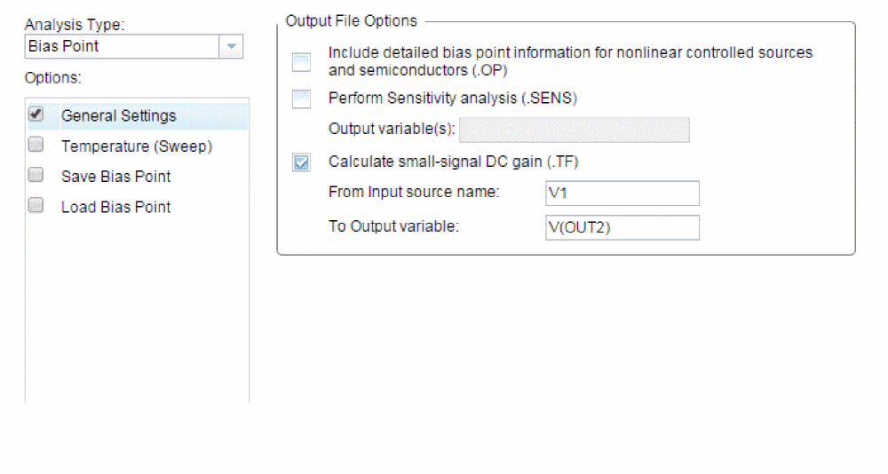
DC sensitivity
Minimum requirements to run a DC sensitivity analysis
Minimum circuit design requirements
None.
Minimum program setup requirements
- In the Bias Point dialog box, select Perform Sensitivity analysis (.SENS).
- Enter the required value(s) in the Output variable(s) box.
- Click OK to save the simulation profile. (Be sure you give the new profile an appropriate name under the General tab prior to saving.)
- In Capture, from the PSpice menu, select Run to start the simulation.
Overview of DC sensitivity
DC sensitivity analysis calculates and reports the sensitivity of one node voltage to each device parameter for the following device types:
- resistors
- independent voltage and current sources
- voltage and current-controlled switches
- diodes
- bipolar transistors
The sensitivity is calculated by linearizing all devices around the bias point. Purely digital devices hold the states calculated when solving for the bias point as discussed in Small-signal DC transfer.
- In this guide, design entry tool is used for both OrCAD X Capture and Design Entry HDL. Any differences between the two tools is mentioned if necessary. Depending on the license available, you will access either PSpice A/D or PSpice Simulator.
View the next document: 10 - AC Sweep and Noise Analysis
If you have any questions or comments about the OrCAD X platform, click on the link below.
Contact Us