07 - Digital Models for Circuit Simulation
Introduction
The standard part libraries contain a comprehensive set of digital parts in many different technologies. Each digital part is described electrically by a digital device model in the form of a subcircuit definition stored in a model library. The corresponding subcircuit name is defined by the part's MODEL attribute value. Other attributes—MNTYMXDLY, IO_LEVEL, and the PSPICEDEFAULTNET set—are passed to the subcircuit, thus providing a high-level means for influencing the behavior of the digital device model.
Generally, the digital parts provided in the part libraries are satisfactory for most circuit designs. However, if your design requires digital parts that are not already provided in the PSpice A/D part and model libraries, you need to define digital device models corresponding to the new digital parts.
A complete digital device model has three main characteristics:
- Functional behavior: described by the gate-level and behavioral digital primitives comprising the subcircuit.
- I/O behavior: described by the I/O model, interface subcircuits, and power supplies related to a logic family.
- Timing behavior: described by one or more timing models, pin-to-pin delay primitives, or constraint checker primitives.
These characteristics are described in this chapter with a running example demonstrating the use of gate-level primitives.
Functional behavior
A digital device model's functional behavior is defined by one or more interconnected digital primitives. Typically, a logic diagram in a data book can be implemented directly using the primitives provided by PSpice A/D. The table below provides a summary of the digital primitives.
| Type | Description |
|---|---|
| Standard gates | |
|
BUF INV AND NAND OR NOR XOR NXOR BUFA INVA ANDA NANDA ORA NORA XORA NXORA AO OA AOI OAI |
buffer inverter AND gate NAND gate OR gate NOR gate exclusive OR gate exclusive NOR gate buffer array inverter array AND gate array NAND gate array OR gate array NOR gate array exclusive OR gate array exclusive NOR gate array AND-OR compound gate OR-AND compound gate AND-NOR compound gate OR-NAND compound gate |
| Tristate gates | |
|
BUF3 INV3 AND3 NAND3 OR3 NOR3 XOR3 NXOR3 BUF3A INV3A AND3A NAND3A OR3A NOR3A XOR3A NXOR3A |
buffer inverter AND gate NAND gate OR gate NOR gate exclusive OR gate exclusive NOR gate buffer array inverter array AND gate array NAND gate array OR gate array NOR gate array exclusive OR gate array exclusive NOR gate array |
| Bidirectional transfer gates | |
|
NBTG PBTG |
N-channel transfer gate P-channel transfer gate |
| Flip-flops and latches | |
|
JKFF DFF SRFF DLTCH |
J-K, negative-edge triggered D-type, positive-edge triggered S-R gated latch D gated latch |
| Pullup/pulldown resistors | |
|
PULLUP PULLDN |
pullup resistor array pulldown resistor array |
| Delay lines | |
|
DLYLINE |
delay line |
| Programmable logic arrays | |
|
PLAND PLOR PLXOR PLNAND PLNOR PLNXOR PLANDC PLORC PLXORC PLNANDC PLNORC PLNXORC |
AND array OR array exclusive OR array NAND array NOR array exclusive NOR array AND array, true and complement OR array, true and complement exclusive OR array, true and complement NAND array, true and complement NOR array, true and complement exclusive NOR array, true and complement |
| Memory | |
|
ROM RAM |
read-only memory random access read-write memory |
|
Multi-Bit A/D & D/A Converters |
|
|
ADC DAC |
multi-bit A/D converter multi-bit D/A converter |
| Behavioral | |
|
LOGICEXP PINDLY CONSTRAINT |
logic expression pin-to-pin delay constraint checking |
The format for digital primitives is similar to that for analog devices. One difference is that most digital primitives require two models instead of one:
- The timing model, which specifies propagation delays and timing constraints such as setup and hold times.
- The I/O model, which specifies information specific to the device's input/output characteristics.
The reason for having two models is that, while timing information is specific to a device, the input/output characteristics are specific to a whole logic family. Thus, many devices in the same family reference the same I/O model, but each device has its own timing model.
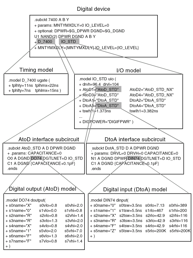
The Figure 7-1 presents an overview of a digital device definition in terms of its primitives and underlying model attributes. These models are discussed further on Timing model and Input/Output model.
Digital primitive syntax
The general digital primitive format is shown below. For specific information on each primitive type see the PSpice A/D Reference Guide. Note that some digital primitives, such as pullups, do not have Timing models. See Timing model for more information.
U<name> <primitive type> [( <parameter value>* )]
+ <digital power node> <digital ground node>
+ <node>*
+ <Timing Model name> <I/O Model name>
+ [MNTYMXDLY=<delay select value>]
+ [IO_LEVEL=<interface subckt select value>]
where
<primitive type> [( <parameter value>* )]
is the type of digital device, such as NAND, JKFF, or INV. It is followed by zero or more parameters specific to the primitive type, such as number of inputs. The number and meaning of the parameters depends on the primitive type.
<digital power node> <digital ground node>
are the nodes used by the interface subcircuits which connect analog nodes to digital nodes or vice versa.
<node>*
is one or more input and output nodes. The number of nodes depends on the primitive type and its parameters. Analog devices, digital devices, or both may be connected to a node. If a node has both analog and digital connections, then PSpice A/D automatically inserts an interface subcircuit to translate between digital output states and voltages.
<Timing model name>
is the name of a timing model that describes the device's timing characteristics, such as propagation delay and setup and hold times. Each timing parameter has a minimum, typical, and maximum value which may be selected during analysis setup.
This type of Timing model and its parameters are specific to each primitive type and are discussed in the PSpice A/D Reference Guide.
<I/O model name>
is the name of an I/O model that describes the device's loading and driving characteristics. I/O models also contain the names of up to four DtoA and AtoD interface subcircuits, which are automatically called by PSpice A/D to handle analog/digital interface nodes. See Input/Output model for more information.
Figure 7-1 Elements of a digital device definition
MNTYMXDLY
is an optional device parameter that selects either the minimum, typical, or maximum delay values from the device's timing model. If not specified, MNTYMXDLY defaults to 0. Valid values are:
|
0 |
= |
the current value of the circuit-wide |
|
1 |
= |
minimum |
|
2 |
= |
typical |
|
3 |
= |
maximum |
|
4 |
= |
worst-case timing (min-max) |
IO_LEVEL
is an optional device parameter that selects one of the four AtoD or DtoA interface subcircuits from the device's I/O model. PSpice A/D calls the selected subcircuit automatically in the event a node connecting to the primitive also connects to an analog device. If not specified, IO_LEVEL defaults to 0. Valid values are:
|
0 |
= |
the current value of the circuit-wide |
|
1 |
= |
AtoD1/DtoA1 |
|
2 |
= |
AtoD2/DtoA2 |
|
3 |
= |
AtoD3/DtoA3 |
|
4 |
= |
AtoD4/DtoA4 |
Following are some simple examples of “U” device declarations:
U1 NAND(2) $G_DPWR $G_DGND 1 2 10 D0_GATE IO_DFT
U2 JKFF(1) $G_DPWR $G_DGND 3 5 200 3 3 10 2 D_293ASTD
+ IO_STD
U3 INV $G_DPWR $G_DGND IN OUT D_INV IO_INV MNTYMXDLY=3
+ IO_LEVEL=2
For example, the 74393 part could be defined as a subcircuit composed of “U” devices as shown below.
.subckt 74393 A CLR QA QB QC QD
+ optional: DPWR=$G_DPWR DGND=$G_DGND
+ params: MNTYMXDLY=0 IO_LEVEL=0
UINV inv DPWR DGND
+ CLR CLRBAR D0_GATE IO_STD
+ IO_LEVEL={IO_LEVEL}
U1 jkff(1) DPWR DGND
+ $D_HI CLRBAR A $D_HI $D_HI
+ QA_BUF $D_NC D_393_1 IO_STD
+ MNTYMXDLY={MNTYMXDLY}
+ IO_LEVEL={IO_LEVEL}
U2 jkff(1) DPWR DGND
+ $D_HI CLRBAR QA_BUF $D_HI $D_HI
+ QB_BUF $D_NC D_393_2 IO_STD
+ MNTYMXDLY={MNTYMXDLY}
U3 jkff(1) DPWR DGND
+ $D_HI CLRBAR QB_BUF $D_HI $D_HI
+ QC_BUF $D_NC D_393_2 IO_STD
+ MNTYMXDLY={MNTYMXDLY}
U4 jkff(1) DPWR DGND
+ $D_HI CLRBAR QC_BUF $D_HI $D_HI
+ QD_BUF $D_NC D_393_3 IO_STD
+ MNTYMXDLY={MNTYMXDLY}
UBUFF bufa(4) DPWR DGND
+ QA_BUF QB_BUF QC_BUF QD_BUF
+ QA QB QC QD D_393_4 IO_STD
+ MNTYMXDLY={MNTYMXDLY}
+ IO_LEVEL={IO_LEVEL}
.ends
When adding digital parts to the part libraries, you must create corresponding digital device models by connecting U devices in a subcircuit definition similar to the one shown above. You should save these in your own custom model library, which you can then configure for use with a given design.
Timing characteristics
A digital device model's timing behavior can be defined in one of two ways:
- Most primitives have an associated Timing model, in which propagation delays and timing constraints (such as setup/hold times) are specified. This method is used when it is easy to partition delays among individual primitives; typically when the number of primitives is small.
- Use the PINDLY and CONSTRAINT primitives, which can directly model pin-to-pin delays and timing constraints for the whole device model. With this method, all other functional primitives operate in zero delay. Refer to the PSpice A/D Reference Guide for a detailed discussion on these two primitives.
In addition to explicit propagation delays, other factors, such as output loads, can affect the total propagation delay through a device.
Timing model
With the exception of the PULLUP, PULLDN, and PINDLY devices, all digital primitives have a Timing model which provides timing parameters to the simulator. The Timing model for each primitive type is unique. That is, the model name and the parameters that can be defined for that model vary with the primitive type.
Within a Timing model, there may be one or more types of parameters:
- Propagation delays (TP)
- Setup times (TSU)
- Hold times (TH)
- Pulse widths (TW)
- Switching times (TSW)
Each parameter is further divided into three values: minimum (MN), typical (TY), and maximum (MX). For example, the typical low-to-high propagation delay on a gate is specified as the parameter TPLHTY. The minimum data-to-clock setup time on a flip-flop is specified as the parameter TSUDCLKMN.
Several timing models are used by digital device 74393 from the model libraries. One of them, D_393_1, is shown below for an edge-triggered flip-flop.
.model D_393_1 ueff (
+ tppcqhlty=18ns tppcqhlmx=33ns
+ tpclkqlhty=6ns tpclkqlhmx=14ns
+ tpclkqhlty=7ns tpclkqhlmx=14ns
+ twclkhmn=20ns twclklmn=20ns
+ twpclmn=20ns tsudclkmn=25ns
+ )
When creating your own digital device models, you can create Timing models like these for the primitives you are using. PSpice A/D recommends that you save these in your own custom model library, which you can then configure for use with a given design.
One or more parameters may be missing from the Timing model definition. Data books do not always provide all three (minimum, typical, and maximum) timing specifications. The way the simulator handles missing parameters depends on the type of parameter.
For a description of Timing model parameters, see the specific primitive type under U devices in the PSpice A/D Reference Guide.
Treatment of unspecified propagation delays
Often, only the typical and maximum delays are specified in data books. If, in this case, the simulator were to assume that the unspecified minimum delay defaults to zero, the logic in certain circuits could break down.
For this reason, the simulator provides two configurable options, DIGMNTYSCALE and DIGTYMXSCALE, which are used to extrapolate unspecified propagation delays in the Timing models.
DIGMNTYSCALE
This option computes the minimum delay when a typical delay is known, using the formula:
TPxxMN = DIGMNTYSCALE ⋅ TPxxTY
DIGMNTYSCALE defaults to the value 0.4, or 40% of the typical delay. Its value must be between 0.0 and 1.0.
DIGTYMXSCALE
This option computes the maximum delay from a typical delay, using the formula
TPxxMX = DIGTYMXSCALE ⋅ TPxxTY
DIGTYMXSCALE defaults to the value 1.6. Its value must be greater than 1.0.
When a typical delay is unspecified, its value is derived from the minimum and/or maximum delays, in one of the following ways. If both the minimum and maximum delays are known, the typical delay is the average of these two values. If only the minimum delay is known, the typical delay is derived using the value of the DIGMNTYSCALE option. Likewise, if only the maximum delay is specified, the typical delay is derived using DIGTYMXSCALE. Obviously, if no values are specified, all three delays will default to zero.
Treatment of unspecified timing constraints
The remaining timing constraint parameters are handled differently than the propagation delays. Often, data books state pulse widths, setup times, and hold times as a minimum value. These parameters do not lend themselves to the extrapolation method used for propagation delays.
Instead, when one or more timing constraints are omitted, the simulator uses the following steps to fill in the missing values:
- If the minimum value is omitted, it defaults to zero.
- If the maximum value is omitted, it takes on the typical value if one was specified, otherwise it takes on the minimum value.
- If the typical value is omitted, it is computed as the average of the minimum and maximum values.
Propagation delay calculation
The timing characteristics of digital primitives are determined by both the timing models and the I/O models. Timing models specify propagation delays and timing constraints such as setup and hold times. I/O models specify input and output loading, driving resistances, and switching times.
When a device's output connects to another digital device, the total propagation delay through a device is determined by adding the loading delay (on the output terminal) to the delay specified in the device's timing model. Loading delay is calculated from the total load on the output and the device's driving resistances. The total load on an output is found by summing the output and input loads (OUTLD and INLD in the I/O model) of all devices connected to that output. This total load, combined with the device's driving resistances (DRVL and DRVH in the I/O model), allows the loading delay to be calculated:
Loading delay = RDRIVE·CTOTAL·ln(2)
The loading delay is calculated for each output terminal of every device before the simulation begins. The total propagation delay is easily calculated during the simulation by adding the pre-calculated loading delay to the device's timing delay. However, for any individual timing delay specification (e.g., TPLH) having a value of 0, the loading delay is not used.
When outputs connect to analog devices, the propagation delay is reduced by the switching times specified in the I/O model. See Input/Output characteristics for more information.
Inertial and transport delay
The simulator uses two different types of internal delay functions when simulating the digital portion of the circuit: inertial delay and transport delay. The application of these concepts is embodied within the implementation of the digital primitives within the simulator. Therefore, they are not user-selectable.
Inertial delay
The simulation of a device may be described as the application of some stimulus (S) to a function (F) and predicting the response (R).
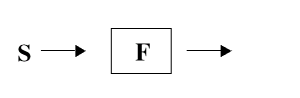
If this device is electrical in nature, application of the stimulus implies that energy will be imparted to the device to cause it to change state. The amount of such energy is a function of the signal's amplitude and duration. If the stimulus is applied to the device for a length of time that is too short, the device will not switch. The minimum duration required for an input change to have an effect on a device's output state is called the inertial delay of the device. For digital simulation, all delay parameters specified in timing models are considered inertial, with the exception of the delay line primitive, DLYLINE.
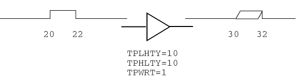
To model the noise immunity behavior of digital devices correctly, the TPWRT (pulse width rejection threshold) parameter can be set in the digital device's I/O model. When pulse width ≥ TPWRT and pulse width < propagation delay, then the device generates either a 0-R-0, 1-F-1, or an X pulse.
This example shows normal operation in which a pulse of 20 nsec width is applied to a BUF primitive having propagation delays of 10 nsec. TPWRT is not set.
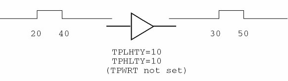
The same device with a short pulse applied produces no output change.
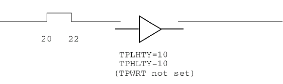
However, if TPWRT is assigned a numerical value (1 or 2 for this example), then the device outputs a glitch.
Transport delay
The delay line primitive is the only simulator model that can propagate any width pulse applied to its input. Its function is to skew the applied stimulus by some constant time value. For example:
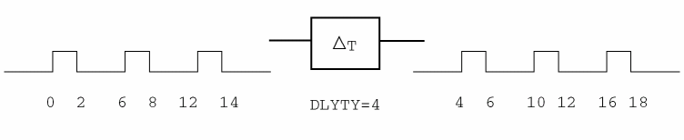
See the DLYLINE digital primitive in the PSpice A/D Reference Guide.
Input/Output characteristics
A digital device model's input/output characteristics are defined by the I/O model that it references. Some characteristics, such as output drive resistance and loading capacitances, apply to digital simulation. Others, such as the interface subcircuits and the power supplies, apply only to mixed analog/digital simulation.
This section describes in detail:
- the I/O model
- the relationship between drive resistances and output strengths
- charge storage on digital nets
- the format of the interface subcircuits
Input/Output model
I/O models are common to entire logic families. For example, in the model libraries, there are only four I/O models for the entire 74LS family: IO_LS, for standard inputs and outputs; IO_LS_OC, for standard inputs and open-collector outputs; IO_LS_ST, for Schmitt trigger inputs and standard outputs; and IO_LS_OC_ST, for Schmitt trigger inputs and open-collector outputs. In contrast, timing models are unique to each device.
I/O models are specified as
.MODEL <I/O model name> UIO [model parameters]*
where valid model parameters are described in Table 7-2.
INLD and OUTLD
These are used in the calculation of loading capacitance, which factors into the propagation delay discussed under timing models on Timing model. Note that INLD does not apply to stimulus generators because they have no input nodes.
DRVH and DRVL
These are used to determine the strength of the output. Strengths are discussed on Defining Output Strengths.
DRVZ, INR, and TSTOREMN
These are used to determine which nets should be simulated as charge storage nets. These are discussed in Charge storage nets.
TPWRT
This is used to specify the pulse width above which the noise immunity behavior of a device is to be considered. See Inertial delay on inertial delay for detail.
The following UIO model parameters are needed only when creating models for use in mixed-signal simulations, and therefore only apply to PSpice simulations.
AtoD1 through AtoD4, and DtoA1 through DtoA4
These are used to hold the names of interface subcircuits. Note that AtoD1 through AtoD4 do not apply to stimulus generators because digital stimuli have no input nodes.
DIGPOWER
This is used to specify the name of the digital power supply PSpice A/D should call if one of the AtoD or DtoA interface subcircuits is called.
TSWLHn and TSWHLn
These switching times are subtracted from a device's propagation delay on the outputs which connect to interface nodes. This compensates for the time it takes the DtoA device to change its output voltage from its current level to that of the switching threshold. By subtracting the switching time from the propagation delay, the analog signal reaches the switching threshold at the correct time (that is, at the exact time of the digital transition). The values for these model parameters should be obtained by measuring the time it takes the analog output of the DtoA (with a nominal analog load attached) to change to the switching threshold after its digital input changes. If the switching time is larger than the propagation delay for an output, no warning is issued, and a delay of zero is used.
When creating your own digital device models, you can create I/O models like these for the primitives you are using. We recommend that you save these in your own custom model library, which you can then configure for use with a given design.
See the PSpice A/D Reference Guide for more information on units and defaults for these parameters.
| UIO model parameter | Description |
|---|---|
|
INLD |
input load capacitance |
|
OUTLD |
output load capacitance |
|
DRVH |
output high level resistance |
|
DRVL |
output low level resistance |
|
DRVZ |
output Z-state leakage resistance |
|
INR |
input leakage resistance |
|
TSTOREMN |
minimum storage time for net to be simulated as a charge |
|
TPWRT |
pulse width rejection threshold |
|
AtoD1 (Level 1) |
name of AtoD interface subcircuit |
|
DtoA1 (Level 1) |
name of DtoA interface subcircuit |
|
AtoD2 (Level 2) |
name of AtoD interface subcircuit |
|
DtoA2 (Level 2) |
name of DtoA interface subcircuit |
|
AtoD3 (Level 3) |
name of AtoD interface subcircuit |
|
DtoA3 (Level 3) |
name of DtoA interface subcircuit |
|
AtoD4 (Level 4) |
name of AtoD interface subcircuit |
|
DtoA4 (Level 4) |
name of DtoA interface subcircuit |
|
DIGPOWER |
name of power supply subcircuit |
|
TSWLH1 |
switching time low to high for DtoA1 |
|
TSWLH2 |
switching time low to high for DtoA2 |
|
TSWLH3 |
switching time low to high for DtoA3 |
|
TSWLH4 |
switching time low to high for DtoA4 |
|
TSWHL1 |
switching time high to low for DtoA1 |
|
TSWHL2 |
switching time high to low for DtoA2 |
|
TSWHL3 |
switching time high to low for DtoA3 |
|
TSWHL4 |
switching time high to low for DtoA4 |
The digital primitives comprising the 74393 part reference the IO_STD I/O model in the model libraries as shown:
.model IO_STD uio (
+ drvh=96.4 drvl=104
+ AtoD1="AtoD_STD" AtoD2="AtoD_STD_NX"
+ AtoD3="AtoD_STD" AtoD4="AtoD_STD_NX"
+ DtoA1="DtoA_STD" DtoA2="DtoA_STD"
+ DtoA3="DtoA_STD" DtoA4="DtoA_STD"
+ tswhl1=1.373ns tswlh1=3.382ns
+ tswhl2=1.346ns tswlh2=3.424ns
+ tswhl3=1.511ns tswlh3=3.517ns
+ tswhl4=1.487ns tswlh4=3.564ns
+ )
Defining Output Strengths
The goal of running simulations is to calculate values for each node in the circuit. For analog nodes, the values are voltages. For digital nodes, these values are states. The state of a digital node is calculated from the output strengths of the devices driving the node and the logic level of the node.
The purpose of strengths is to allow the simulator to find the value of a node when more than one output is driving it. A common example is a bus line which is driven by more than one tristate driver. Under normal circumstances, all drivers except one are driving at the Z (high impedance) strength. Thus, the bus line will take on the value of the one gate that is driving at a higher strength (lower impedance).
Another example is a bus line connected to several open collector output devices and a digital pullup resistor. The pullup resistor outputs a 1 level at a weak (but non-Z) strength. If all of the open-collector devices are outputting at Z strength, then the node will have a 1 level because of the pullup resistor. If any of the open collectors output a 0, at a higher strength than the pullup resistor, then the 0 will overpower the weak 1 from the pullup, and the node will be a 0 level.
Parts with open collector configuration need to be driven by external pullup or pulldown resistors to drive to 1 or 0 states.
Configuring the strength scale
The 64 strengths are determined by two configurable options: DIGDRVZ and DIGDRVF. You can set these options in the Simulation Settings dialog box in PSpice A/D.
DIGDRVZ defines the impedance of the Z strength, and DIGDRVF defines the impedance of the forcing strength. These two values define a logarithmic scale consisting of 64 ranges of impedance values. By default, DIGDRVZ is 20 kohms and DIGDRVF is 2 ohms. The larger the range between DIGDRVZ and DIGDRVF, the larger the range of impedance values in each of the 64 strengths.
Determining the strength of a device output
The simulator uses the value of the DRVH (high-level driving resistance) or DRVL (low-level driving resistance) parameters from the device's I/O model. If the level of the output is a 1, the simulator obtains the strength by finding the bin which contains the value of the DRVH parameter. Likewise, if the level is a 0, the simulator uses the value of the DRVL parameter to obtain the strength.
See Input/Output model for more information.
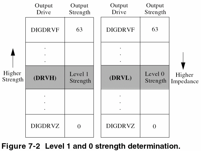
Note that if the values of DRVH and DRVL in the I/O model are different, it is possible for the 1 and 0 levels to have different strengths. This is useful for open-collector devices, where the 0 level is at a higher strength than the 1 level (which drives at the Z strength).
Drive impedances which are higher than the value of DIGDRVZ are assigned the Z strength (0). Likewise, drive impedances lower than the value of DIGDRVF are assigned the forcing strength (63).
Controlling overdrive
During a simulation, the simulator uses only the strength range number (0-63) to compare the driving strength of outputs. The simulator allows you to control how much stronger an output must be before it overdrives the other outputs driving the same node. This is controlled with the configurable DIGOVRDRV option. By default, DIGOVRDRV is 3, meaning that the strength value assigned to an output must be at least 3 greater than all other drivers before it determines the level of the node.
The accuracy of the DIGOVRDRV strength comparison is limited by the size of the strength range, DIGDRVZ through DIGDRVF. The default drive range of 2 ohms to 20,000 ohms gives strength ranges of 7.5%. The accuracy of the strength comparison is 15%. In other words, depending on the particular values of DRVH and DRVL, it might take as much as a factor of 3.45 to overdrive a signal, or as little as a factor of 2.55. The accuracy of the comparison increases as the ratio between DIGDRVF and DIGDRVZ decreases.
You can set the DRVH, DRVL, DIGDRVF, DIGDRVZ, and DIGOVRDRV options in the Simulation Settings dialog box in PSpice A/D.
Charge storage nets
The ability to model charge storage on digital nets is useful for engineers who are designing dynamic MOS integrated circuits. In such circuits, it is common for the designer to temporarily store a one or zero on a net by driving the net to the appropriate voltage and then turning off the drive. The charge which is trapped on the net causes the net's voltage to remain unchanged for some time after the net is no longer driven. The technique is not normally used on PCB nets because sub-nanoampere input and output leakage currents would be required, as well as low coupling from adjacent signals.
The simulator models the stored charge nets using a simplified switch-level simulation technique. A normalized (with respect to power supply) charge or discharge current is calculated for each output or transfer gate attached to the net. This current, divided by the net's total capacitance, is integrated and recalculated at intervals which are appropriate for the particular net. The net's digital level is determined by the normalized voltage on the net. Only the digital level (1, 0, R, F, X) on the net is used by device inputs attached to the net.
This technique allows accurate simulation of networks of transfer gates and capacitive loads. The sharing of charge among several nets which are connected by transfer gates is handled properly because the simulation method calculates the charge transferred between the nets, and maintains a floating-point value for the charge on the net (not just a one or zero). Because of the increased computation, it takes the simulator longer to simulate charge storage nets than normal digital nets. However, charge storage nets are simulated much faster than analog nets.
The I/O model parameters INR, DRVZ, and TSTOREMN (see Table 7-2) are used by the simulator to determine which nets should be simulated as charge storage nets. The simulator will simulate charge storage only for a net which has some devices attached to it which can be high impedance (Z), and which has a storage time greater than or equal to the smallest TSTOREMN of all inputs attached to the net. The storage time is calculated as the total capacitance (sum of all INLD and OUTLD values for attached inputs and outputs) multiplied by the total leakage resistance for the net (the parallel combination of all INR and DRVZ values for attached inputs and outputs).
Creating your own interface subcircuits for additional technologies
If you are creating custom digital parts for a technology which is not in the model libraries, you may also need to create AtoD and DtoA subcircuits. The new subcircuits need to be referenced by the I/O models for that technology. The AtoD and DtoA interfaces have specific formats, such as node order and parameters, which are expected by PSpice A/D for mixed-signal simulations.
If you are creating parts in one of the logic families already in the model libraries, you should reference the existing I/O models appropriate to that family. The I/O models, in turn, automatically reference the correct interface subcircuits for that family. These, too, are already contained in the model libraries.
The AtoD interface subcircuit format is shown here:
.SUBCKT ATOD <name suffix>
+ <analog input node>
+ <digital output node>
+ <digital power supply node>
+ <digital ground node>
+ PARAMS: CAPACITANCE=<input load value>
+ {O device, loading capacitor, and other
+ declarations}
.ENDS
It has four nodes as described. The AtoD subcircuit has one parameter, CAPACITANCE, which corresponds to the input load. PSpice A/D passes the value of the I/O model parameter INLD to this parameter when the interface subcircuit is called.
The DtoA interface subcircuit format is shown here:
.SUBCKT DTOA <name suffix>
+ <digital input node> <analog output node>
+ <digital power supply node> <digital
+ ground node>
+ PARAMS: DRVL=<0 level driving resistance>
+ DRVH=<1 level driving resistance>
+ CAPACITANCE=<output load value>
+ {N device, loading capacitor, and other
+ declarations}
.ENDS
It also has four nodes. Unlike the AtoD subcircuit, the DtoA subcircuit has three parameters. PSpice A/D will pass the values of the I/O model parameters DRVL, DRVH, and OUTLD to the interface subcircuit's DRVL, DRVH, and CAPACITANCE parameters when it is called.
The library file DIG_IO.LIB contains the I/O models and interface subcircuits for all logic families supported in the model libraries. You should refer to this file for examples of the I/O models, interface subcircuits, and the proper use of N and O devices.
Shown below are the I/O model and AtoD interface subcircuit definition used by the primitives describing the 74393 part.
.model IO_STD uio (
+ drvh=96.4 drvl=104
+ AtoD1="AtoD_STD" AtoD2="AtoD_STD_NX"
+ AtoD3="AtoD_STD" AtoD4="AtoD_STD_NX"
+ DtoA1="DtoA_STD" DtoA2="DtoA_STD"
+ DtoA3="DtoA_STD" DtoA4="DtoA_STD"
+ tswhl1=1.373 tswlh1=3.382ns
+ tswhl2=1.346ns tswlh2=3.424ns
+ tswhl3=1.511ns tswlh3=3.517ns
+ tswhl4=1.487ns tswlh4=3.564ns
+ )
.subckt AtoD_STD A D DPWR DGND
+ params: CAPACITANCE=0
*
O0 A DGND DO74 DGTLNET=D IO_STD
C1 A 0 {CAPACITANCE+0.1pF}
.ends
If an instance of the 74393 part is connected to an analog part via node AD_NODE, PSpice A/D generates an interface block using the I/O model specified by the digital primitive actually at the interface. Suppose that U1 is the primitive connected at AD_NODE (see the 74393 subcircuit definition on page 393), and that the IO_LEVEL is set to 1. PSpice A/D determines that IO_STD is the I/O model used by U1. Notice how IO_STD identifies the interface subcircuit names AtoD_STD and DtoA_STD to be used for level 1 subcircuit selection. If the connection with U1 is an input (such as a clock line), PSpice A/D creates an instance of the subcircuit AtoD_STD:
X$AD_NODE_AtoD1 AD_NODE AD_NODE$AtoD $G_DPWR
+ $G_DGND
+ AtoD_STD
+ PARAMS: CAPACITANCE=0
The AtoD_STD interface subcircuit references the DO74 model in its PSpice O device declaration. This model, stated elsewhere in the model libraries, describes how to translate an analog signal on the analog side of an interface node, to a digital state on the digital side of an interface node.
.model DO74 doutput
+ s0name="X" s0vlo=0.8 s0vhi=2.0
+ s1name="0" s1vlo=-1.5 s1vhi=0.8
+ s2name="R" s2vlo=0.8 s2vhi=1.4
+ s3name="R" s3vlo=1.3 s3vhi=2.0
+ s4name="X" s4vlo=0.8 s4vhi=2.0
+ s5name="1" s5vlo=2.0 s5vhi=7.0
+ s6name="F" s6vlo=1.3 s6vhi=2.0
+ s7name="F" s7vlo=0.8 s7vhi=1.4
+
The DOUTPUT model parameters are described under O devices in the PSpice A/D Reference Guide.
Supposing the output of the 74393 is connected to an analog part via the digital primitive UBUFF. At IO_LEVEL set to 1, PSpice A/D determines that the DtoA_STD interface subcircuit identified in the IO_STD model, should be used.
.subckt DtoA_STD D A DPWR DGND
+ params: DRVL=0 DRVH=0 CAPACITANCE=0
*
N1 A DGND DPWR DIN74 DGTLNET=D IO_STD
C1 A DGND {CAPACITANCE+0.1pF}
.ends
For this subcircuit, the DRVH and DRVL parameters values specified in the IO_STD model would be passed to it. (The interface subcircuits in the model libraries do not currently use these values.)
The DtoA_STD interface subcircuit references the DIN74 model in its PSpice N device declaration. This model, stated elsewhere in the libraries, describes how to translate a digital state into a voltage and impedance.
.model DIN74 dinput (
+ s0name="0" s0tsw=3.5ns s0rlo=7.13
+ s0rhi=389 ; 7ohm, 0.09v
+ s1name="1" s1tsw=5.5ns s1rlo=467
+ s1rhi=200 ; 140ohm, 3.5v
+ s2name="X" s2tsw=3.5ns s2rlo=42.9
+ s2rhi=116 ; 31.3ohm, 1.35v
+ s3name="R" s3tsw=3.5ns s3rlo=42.9
+ s3rhi=116 ; 31.3ohm, 1.35v
+ s4name="F" s4tsw=3.5ns s4rlo=42.9
+ s4rhi=116 ; 31.3ohm, 1.35v
+ s5name="Z" s5tsw=3.5ns s5rlo=200K
+ s5rhi=200K
+)
The DINPUT model parameters are described under PSpice N devices in the PSpice A/D Reference Guide.
Each state is turned into a pullup and pulldown resistor pair to provide the correct voltage and impedance. The Z state is accounted for as well as the 0, 1, and X logic levels.
You can create your own interface subcircuits, DINPUT models, DOUTPUT models, and I/O models like these for technologies not currently supported in the model libraries. We recommend that you save these in your own custom model library, which you can then configure for use with a given design.
Creating a digital model using the PINDLY and LOGICEXP primitives
Unlike the majority of analog device types, the bulk of digital devices are not primitives that are compiled into the simulator. Instead, most digital models are macro models or subcircuits that are built from a few primitive devices.
These subcircuits reference interface and timing models to handle the D-to-A and A-to-D interfaces and the overall timing parameters of the physical device. For most families of digital components, the interface models are already defined and available in the DIG_IO.LIB library, which is supplied with all digital and mixed-signal packages. If you are unsure of the exact name of the interface model you need to use, use a text editor to look in DIG_IO.LIB.
For instance, if you are trying to model a 74LS component that is not already in a library, open DIG_IO.LIB with your text editor and search for 74LS to get the interface models for the 74LS family. You can also read the information at the beginning of the file which explains many of the terms and uses for the I/O models.
In the past, the timing model has presented the greatest challenge when trying to model a digital component. This was due to the delays of a component being distributed among the various gates. Recently, the ability to model digital components using logic expressions (LOGICEXP) and pin-to-pin delays (PINDLY) has been added to the simulator. Using the LOGICEXP and PINDLY digital primitives, you can describe the logic of the device with zero delay and then enter the timing parameters for the pin-to-pin delays directly from the manufacturer's data sheet. Digital primitives still must reference a standard timing model, but when the PINDLY device is used, the timing models are simply zero-delay models that are supplied in DIG_IO.LIB. The default timing models can be found in the same manner as the standard I/O models. The PINDLY primitive also incorporates constraint checking which allows you to enter device data such as pulse width and setup/hold timing from the data sheet. Then the simulator can verify that these conditions are met during the simulation.
Digital primitives
Primitives in the simulator are devices or functions which are compiled directly into the code. The primitives serve as fundamental building blocks for more complex macro models.
There are two types of primitives in the simulator: gate level and behavioral. A gate level primitive normally refers to an actual physical device (such as buffers, AND gates, inverters). A behavioral primitive is not an actual physical device, but rather helps to define parameters of a higher level model. Just like gate level primitives, behavioral primitives are intrinsic functions in the simulator and are treated in much the same manner. They are included in the gate count for circuit size and cannot be described by any lower level model.
In our 74160 example (see The TTL Data Book from Texas Instruments for schematic and description), the four J-K flip-flops are the four digital gate level primitives. While flip-flops are physically more complex than gates in terms of modeling, they are defined on the same level as a gate (for example, flip-flops are a basic device in the simulator). Since all four share a common Reset, Clear, and Clock signal, they can be combined into one statement as an array of flip-flops. They could just as easily have been written separately, but the array method is more compact. See the Digital Devices chapter in the PSpice A/D Reference Guide for more information.
Logic expression (LOGICEXP primitive)
Looking at the listing in 74160 example and at the schematic representation of the 74160 subcircuit, you can see that there are three main parts to the subcircuit. Following the usual header information, .SUBCKT keyword, subcircuit name, interface pin list, and parameter list is the LOGICEXP primitive. It contains everything in the component that can be expressed in terms of simple combinational logic. The logic expression device also serves to buffer other input signals that will go to the PINDLY primitive. In this case, LOGICEXP buffers the ENP_I, ENT_I, CLK_I, CLRBAR_I, LOADBAR_I, and four data signals. See the Digital Devices chapter in the PSpice A/D Reference Guide for more information.
For our 74160 example, the logic expression (LOGICEXP) has fourteen inputs and twenty outputs. The inputs are the nine interface input pins in the subcircuit plus five feedback signals that come from the flip-flops (QA, QB, QC, QD, and QDBAR). The flip-flops are primitive devices themselves and are not part of the logic expression. The outputs are the eight J-K data inputs to the flip-flops, RCO, the four data lines used internal to the logic expression (A, B, C, D), and the seven control lines: CLK, CLKBAR, EN, ENT, ENP, CLRBAR, and LOADBAR.
The schematic representation of the device shows buffers on every input signal of the model, while the logic diagram of the device in the data book shows buffers or inverters on only the CLRBAR_I, CLK_I, and LOADBAR_I signals. We have added buffers to the inputs to minimize the insertion of A-to-D interfaces when the device is driven by analog circuitry. The best example is the CLK signal. With the buffer in place, if the CLK signal is analog, one A-to-D interface device will be inserted into the circuit by the simulator. If the buffer was not present, then an interface device would be inserted at the CLK pin of each of the flip-flops. The buffers have no delay associated with them, but by minimizing the number of A-to-D interfaces, we speed up the mixed-signal simulation by reducing the number of necessary calculations. For situations where the device is only connected to other digital nodes, the buffers have no effect on the simulation.
The D0_GATE, shown in the listing, is a zero-delay primitive gate timing model. For most TTL modeling applications, this only serves as a place holder and is not an active part of the model. Its function has been replaced by the PINDLY primitive. The D0_GATE model can be found in the library file DIG_IO.LIB. For a more detailed description of digital primitives, see the Digital Devices chapter in the PSpice A/D Reference Guide.
IO_STD, shown in the listing, is the standard I/O model. This determines the A-to-D and D-to-A interface characteristics for the subcircuit. The device contains family-specific information, but the models have been created for nearly all of the stock families. The various I/O models can be found in the library file DIG_IO.LIB.
The logic expressions themselves are straightforward. The first nine are buffering the input signals from outside the subcircuit. The rest describe the logic of the actual device up to the flip-flops. By tracing the various paths in the design, you can derive each of the logic equations.
The D0_EFF timing model, shown in the listing, is a zero-delay default model already defined in DIG_IO.LIB for use with flip-flops. All of the delays for the device are defined in the PINDLY section. The I/O model is IO_STD as identified previously. We have not specified a MNTYMXDLY or IO_LEVEL parameter, so the default values are used. For a more detailed description of the general digital primitives MNTYMXDLY and IO_LEVEL, see the Digital Devices chapter in the PSpice A/D Reference Guide.
The primitive MNTYMXDLY specifies whether to use the minimum, typical, maximum, or digital worst-case timing values from the device's timing model (in this case the PINDLY device). For the 74160, MNTYMXDLY is set to 0. This means that it takes on the current value of the DIGMNTYMX parameter. DIGMNTYMX defaults to 2 (typical timing) unless specifically changed using the .OPTIONS command.
The primitive IO_LEVEL selects one of four possible A-to-D and D-to-A interface subcircuits from the device's I/O model. In the header of this subcircuit, IO_LEVEL is set to 0. This means that it takes on the value of the DIGIOLVL parameter. DIGIOLVL defaults to 1 unless specifically changed using the .OPTIONS command.
Pin-to-pin delay (PINDLY primitive)
The delay and constraint specifications for the model are specified using the PINDLY primitive. The PINDLY primitive is evaluated every time any of its inputs or outputs change. See the Digital Devices chapter in the PSpice A/D Reference Guide for more information.
For the 74160, we have five delay paths, the four flip-flop outputs to subcircuit outputs QA...QD to QA_O...QD_O, and RCO to RCO_O. The five paths are seen in the Delay & Constraint section of the design. For delay paths, the number of inputs must equal the number of outputs. Since the 74160 does not have TRI-STATE outputs, there are no enable signals for this example, but there are ten reference nodes. The first four (CLK, LOADBAR, ENT, and CLRBAR) are used for both the pin-to-pin delay specification and the constraint checking. The last six (ENP, A, B, C, D, and EN) are used only for the constraint checking.
The PINDLY primitive also allows constraint checking of the model. It can verify the setup, hold times, pulse width, and frequency. It also has a general mechanism to allow for user-defined conditions to be reported. The constraint checking only reports timing violations; it does not affect the propagation delay or the logic state of the device. Since the timing parameters are generally specified at the pin level of the actual device, the checking is normally done at the interface pins of the subcircuit after the appropriate buffering has been done.
BOOLEAN
The keyword BOOLEAN begins the boolean assignments which define temporary variables that can be used later in the PINDLY primitive. The form is:
boolean variable = {boolean expression}
The curly braces are required.
In the 74160 model, the boolean expressions are actually reference functions. There are three reference functions available: CHANGED, CHANGED_LH, and CHANGED_HL. The format is:
function name (node, delta time)
For our example, we define the variable CLOCK as a logical TRUE if there has been a LO-to-HI transition of the CLK signal at simulation time. We define CNTENT as TRUE if there has been any transition of the ENT signal at the simulation time.
Boolean operators take the following boolean values as operands:
- reference functions
- transition functions
- previously assigned boolean variables
- boolean constants TRUE and FALSE
Transition functions have the general form of:
TRN_pn
For a complete list of reference functions and transition functions, see the Digital Devices chapter in the PSpice A/D Reference Guide.
PINDLY
PINDLY contains the actual delay and constraint expressions for each of the outputs.
The CASE function defines a more complex, rule-based <delay expression> and works as a rule section mechanism for establishing path delays. Each boolean expression in the CASE function is evaluated in order until one is encountered that produces a TRUE result. Once a TRUE expression is found, the delay expression portion of the rule is associated with the output node being evaluated, and the remainder of the CASE function is ignored. If none of the expressions evaluate to TRUE, then the DEFAULT delay is used. Since it is possible for none of the expressions to yield a TRUE result, you must include a default delay in every CASE function. Also note that the expressions must be separated by a comma.
In the PINDLY section of the PINDLY primitive in the model listing, the four output nodes (QA_O through QD_O) all use the same delay rules. The CASE function is evaluated independently for each of the outputs in turn. The first delay expression is:
CLOCK & LOADBAR=='1 & TRN_LH, DELAY(-1,13NS,20NS)
This means that if CLOCK is TRUE, and LOADBAR is equal to 1, and QA_O is transitioning from 0 to 1, then the values of -1, 13ns, and 20ns are used for the MINIMUM, TYPICAL, and MAXIMUM propagation delay for the CLK-to-QA data output of the chip. In this case, the manufacturer did not supply a minimum prop delay, so we used the value -1 to tell the simulator to derive a value from what was given. If this statement is TRUE, then the simulator assigns the values and move on to the CASE function for QB_O and eventually RCO_O.
For instances where one or more propagation delay parameters are not supplied by the data sheet, the simulator derives a value from what is known and the values specified for the .OPTION DIGMNTYSCALE and DIGTYMXSCALE.
When the typical value for a delay parameter is known but the minimum is not, the simulator uses the formula:
TPxxMN = DIGMNTYSCALE X TPxxTY
where the value of DIGMNTYSCALE is between 0.1 and 1.0 with the default value being 0.4. If the typical is known and the maximum is not, then the simulator uses the formula:
TPxxMX = DIGTYMXSCALE X TPxxTY
where the value of DIGTYMXSCALE is greater than 1.0 with the default being 1.6. If the typical value is not known, and both the minimum and maximum are, then the typical value used by the simulator will be the average of the minimum and maximum propagation delays. If only one of min or max is known, then the typical delay is calculated using the appropriate formula as listed above. If all three are unknown, then they all default to a value of 0.
Constraint checker (CONSTRAINT primitive)
The CONSTRAINT primitive provides a general constraint checking mechanism to the digital device modeler. It performs setup and hold time checks, pulse width checks, frequency checks, and includes a general mechanism to allow user-defined conditions to be reported. See the Digital Devices chapter in the PSpice A/D Reference Guide for more information.
Setup_Hold
The expressions in the SETUP_HOLD specification may be listed in any order.
CLOCK defines the node that is to be used as the reference for the setup/ hold/ release specification. The assertion edge must be LH or HL (for example, a transition from logic state 0 to 1 or from 1 to 0.)
DATA specifies which node(s) is to have its setup/ hold time measured.
SETUPTIME defines the minimum time that all DATA nodes must be stable prior to the assertion edge of the clock. The time value must be a nonnegative constant or expression and is measured in seconds. If the device has different setup/ hold times depending on whether the data is HI or LOW at the clock change, you can use either or both of the following forms:
SETUPTIME_LO = <time value> SETUPTIME_HI = <time value>
If either of the time values is 0, then no check is done for that case.
HOLDTIME is used in the same way as SETUPTIME and also has the alternate _LH and _HL formats and 0 value condition.
RELEASETIME causes the simulator to perform a special-purpose setup check. Release time (also referred to as recovery time in some data sheets) refers to the minimum time that a signal can go inactive before the active clock edge. Again, the _LH and _HL forms are available. The difference between RELEASETIME and SETUPTIME checking is that simultaneous CLOCK/ DATA transitions are never allowed (this assumes a nonzero hold time). RELEASETIME is usually not used in conjunction with SETUPTIME or HOLDTIME.
Width
WIDTH does the minimum pulse-width checking. MIN_HI/ MIN_LO is the minimum time that the node can remain HI/LOW. The value must be a nonnegative constant, or expression. A value of 0 means that any pulse width is allowed. At least one of MIN_HI or MIN_LO must be used within a WIDTH section.
Freq
FREQ checks the frequency. MINFREQ/ MAXFREQ is the minimum/ maximum frequency that is allowed on the node in question. The value must be a nonnegative floating point constant or expression measured in hertz. At least one of MINFREQ or MAXFREQ must be used within a FREQ section.
AFFECTS clauses (not used in this example) can be included in constraints to describe how the simulator should associate the failure of a constraint check with the outputs (paths through the device) of the PINDLY. This information does not affect the logic state of the outputs but provides causality detail used by the error tracking mechanism in PSpice A/D waveform analysis.
74160 example
In the 74160 example, we are checking that the maximum clock frequency (CLK) is not more than 25 MHz and the pulse width is 25 ns. We are also checking that the CLRBAR signal has a minimum LO pulse width of 20 ns, and that the 4 data inputs (A, B, C, D) have a setup/ hold time of 20 ns in reference to the CLK signal. We are also checking that ENP and ENT have a setup/ hold time of 20 ns with respect to the 0 to 1 transition of the CLK signal, but only when the conditions in the WHEN statement are met. All of the delay and constraint checking values were taken directly from the actual data sheet. This makes the delay modeling both easy and accurate.
All of the above primitives and modeling methods, as well as a few special cases that are not covered here, can be found in the Digital Devices chapter of the PSpice A/D Reference Guide.
* 74160 Synchronous 4-bit Decade Counters with asynchronous clear * Modeled using LOGICEXP, PINDLY, & CONSTRAINT devices .SUBCKT 74160 CLK_I ENP_I ENT_I CLRBAR_I LOADBAR_I A_I B_I C_I D_I + QA_O QB_O QC_O QD_O RCO_O + OPTIONAL: DPWR=$G_DPWR DGND=$G_DGND + PARAMS: MNTYMXDLY=0 IO_LEVEL=0 * U160LOG LOGICEXP(14,20) DPWR DGND + CLK_I ENP_I ENT_I CLRBAR_I LOADBAR_I A_I B_I C_I D_I + QDBAR QA QB QC QD + CLK ENP ENT CLRBAR LOADBAR A B C D + CLKBAR RCO JA JB JC JD KA KB KC KD EN + D0_GATE IO_STD IO_LEVEL={IO_LEVEL} + LOGIC: + CLK = { CLK_I } ;Buffering + ENP = { ENP_I } + ENT = { ENT_I } + CLRBAR = { CLRBAR_I } + LOADBAR = { LOADBAR_I } + A = { A_I } + B = { B_I } + C = { C_I } + D = { D_I } + CLKBAR = { ~CLK } ;Logic expressions + LOAD = { ~LOADBAR } + EN = { ENP & ENT } + I1A = { LOAD | EN } + I2A = { ~(LOAD & A) } + JA = { I1A & ~(LOAD & I2A) } + KA = { I1A & I2A } + I1B = { (QA & EN & QDBAR) | LOAD } + I2B = { ~(LOAD & B) } + JB = { I1B & ~(LOAD & I2B) } + KB = { I1B & I2B } + I1C = { (QA & EN & QB) | LOAD } + I2C = { ~(LOAD & C) } + JC = { I1C & ~(LOAD & I2C) } + KC = { I1C & I2C } + I1D = { ((QC & QB & QA & EN) | (EN & QA & QD)) | LOAD } + I2D = { ~(LOAD & D) } + JD = { I1D & ~(LOAD & I2D) } + KD = { I1D & I2D } + RCO = { QD & QA & ENT } * UJKFF JKFF(4) DPWR DGND $D_HI CLRBAR CLKBAR JA JB JC JD KA KB KC KD + QA QB QC QD QABAR QBBAR QCBAR QDBAR D0_EFF IO_STD U160DLY PINDLY (5,0,10) DPWR DGND + RCO QA QB QC QD + CLK LOADBAR ENT CLRBAR ENP A B C D EN + RCO_O QA_O QB_O QC_O QD_O + IO_STD MNTYMXDLY={MNTYMXDLY} IO_LEVEL={IO_LEVEL} + BOOLEAN: + CLOCK = { CHANGED_LH(CLK,0) } + CNTENT = { CHANGED(ENT,0) } + PINDLY: + QA_O QB_O QC_O QD_O = { + CASE( + CLOCK & LOADBAR=='1 & TRN_LH, DELAY(-1,13NS,20NS), + CLOCK & LOADBAR=='1 & TRN_HL, DELAY(-1,15NS,23NS), + CLOCK & LOADBAR=='0 & TRN_LH, DELAY(-1,17NS,25NS), + CLOCK & LOADBAR=='0 & TRN_HL, DELAY(-1,19NS,29NS), + CHANGED_HL(CLRBAR,0), DELAY(-1,26NS,38NS), + DELAY(-1,26NS,38NS) + ) + } + RCO_O = { + CASE( + CNTENT, DELAY(-1,11NS,16NS), + CLOCK, DELAY(-1,23NS,35NS), + DELAY(-1,23NS,35NS) + ) + } + FREQ: + NODE = CLK + MAXFREQ = 25MEG + WIDTH: + NODE = CLK + MIN_LO = 25NS + MIN_HI = 25NS + WIDTH: + NODE = CLRBAR + MIN_LO = 20NS + SETUP_HOLD: + DATA(4) = A B C D + CLOCK LH = CLK + SETUPTIME = 20NS + WHEN = { (LOADBAR!='1 ^ CHANGED(LOADBAR,0)) & + CLRBAR!='0 } + SETUP_HOLD: + DATA(2) = ENP ENT + CLOCK LH = CLK + SETUPTIME = 20NS + WHEN = { CLRBAR!='0 & (LOADBAR!='0 ^ + CHANGED(LOADBAR,0)) + & CHANGED(EN,20NS) } + SETUP_HOLD: + DATA(1) = LOADBAR + CLOCK LH = CLK + SETUPTIME = 25NS + WHEN = { CLRBAR!='0 } + SETUP_HOLD: + DATA(1) = CLRBAR + CLOCK LH = CLK + RELEASETIME_LH = 20NS .ENDS
View the next document: 08 - PSpice Digital Models for Circuit Simulation
If you have any questions or comments about the OrCAD X platform, click on the link below.
Contact Us