06 - Analog Behavioral Modeling
Overview of analog behavioral modeling
You can use the Analog Behavioral Modeling (ABM) feature of PSpice A/D to make flexible descriptions of electronic components in terms of a transfer function or lookup table. In other words, a mathematical relationship is used to model a circuit segment, so you do not need to design the segment component by component.
The part library contains several ABM parts that are classified as either control system parts or as PSpice-equivalent parts. See Basic controlled sources for an introduction to these parts, how to use them, and the difference between parts with general-purpose application and parts with special-purpose application.
Control system parts are defined with the reference voltage preset to ground so that each controlling input and output are represented by a single pin in the part. These are described in Control system parts.
PSpice-equivalent parts reflect the structure of the PSpice E and G device types, which respond to a differential input and have double-ended output. These are described in PSpice-equivalent parts.
You can also use the Device Equations Developer’s Kit for modeling of this type, but we recommend using the ABM feature wherever possible. With the Device Equations Developer’s Kit, the PSpice A/D source code is actually modified. While this is more flexible and produces faster results, it is also much more difficult to use and to troubleshoot. Also, any changes you make using the Device Equations Developer’s Kit must be made to all new PSpice A/D updates you install.
Device models made with ABM can be used for most cases, are much easier to create, and are compatible with PSpice A/D updates.
The ABM part library file
The ABM part library contains the ABM components. This library contains two sections.
The first section has parts that you can quickly connect to form control system types of circuits. These components have names like SUM, GAIN, LAPLACE, and HIPASS.
The second section contains parts that are useful for more traditional controlled source forms of schematic parts. These PSpice-equivalent parts have names like EVALUE and GFREQ and are based on extensions to traditional PSpice E and G device types.
Implement ABM components by using PSpice primitives; there is no corresponding ABM.LIB model library. A few components generate multi-line netlist entries, but most are implemented as single PSpice E or G device declarations. See ABM part templates for a description of PSPICETEMPLATE properties and their role in generating netlist declarations. See Implementation of PSpice-equivalent parts for more information about PSpice E and G syntax.
Placing and specifying ABM parts
Place and connect ABM parts the same way you place other parts. After you place an ABM part, you can edit the instance properties to customize the operational behavior of the part. This is equivalent to defining an ABM expression describing how inputs are transformed into outputs. The following sections describe the rules for specifying ABM expressions.
Net names and device names in ABM expressions
In ABM expressions, refer to signals by name. This is also considerably more convenient than having to connect a wire from a pin on an ABM component to a point carrying the voltage of interest.
If you used an expression such as V(2), then the referenced net (2 in this case) is interpreted as the name of a local or global net. A local net is a labeled wire or bus segment in a hierarchical schematic, or a labeled offpage connector. A global net is a labeled wire or bus segment at the top level, or a global connector.
OrCAD X Capture recognizes these constructs in ABM expressions:
V(<net name>)
V(<net name>,<net name>)
I(<vdevice>)
When one of these is recognized, Capture searches for <net name> or <vdevice> in the net name space or the device name space, respectively. Names are searched for first at the hierarchical level of the part being netlisted. If not found there, then the set of global names is searched. If the fragment is not found, then a warning is issued but Capture still outputs the resulting netlist. When a match is found, the original fragment is replaced by the fully qualified name of the net or device.
For example, suppose we have a hierarchical part U1. Inside the schematic representing U1 we have an ABM expression including the term V(Reference). If “Reference” is the name of a local net, then the fragment written to the netlist will be translated to V(U1_Reference). If “Reference” is the name of a global net, the corresponding netlist fragment will be V(Reference).
Names of voltage sources are treated similarly. For example, an expression including the term I(Vsense) will be output as I(V_U1_Vsense) if the voltage source exists locally, and as I(V_Vsense) if the voltage source exists at the top level.
Forcing the use of a global definition
If a net name exists both at the local hierarchical level and at the top level, the search mechanism used by Capture will find the local definition. You can override this, and force Capture to use the global definition, by prefixing the name with a single quote (') character.
For example, suppose there is a net called Reference both inside hierarchical part U1 and at the top level. Then, the ABM fragment V(Reference) will result in V(U1_Reference) in the netlist, while the fragment V('Reference) will produce V(Reference).
ABM part templates
For most ABM parts, a single PSpice “E” or “G” device declaration is output to the netlist per part instance. The PSPICETEMPLATE property in these cases is straightforward. For example the LOG part defines an expression variant of the E device with its output being the natural logarithm of the voltage between the input pin and ground:
E^@REFDES %out 0 VALUE { LOG(V(%in)) }The fragment E^@REFDES is standard. The “E” specifies a PSpice A/D controlled voltage source (E device); %in and %out are the input and output pins, respectively; VALUE is the keyword specifying the type of ABM device; and the expression inside the curly braces defines the logarithm of the input voltage.
Several ABM parts produce more than one primitive PSpice A/D device per part instance. In this case, the PSPICETEMPLATE property may be quite complicated. An example is the DIFFER (differentiator) part. This is implemented as a capacitor in series with a current sensor together with an E device which outputs a voltage proportional to the current through the capacitor.
The template has several unusual features: it gives rise to three primitives in the PSpice A/D netlist, and it creates a local node for the connection of the capacitor and its current-sensing V device.
C^@REFDES %in $$U^@REFDES 1\n
V^@REFDES $$U^@REFDES 0 0v\n
E^@REFDES %out 0 VALUE {@GAIN * I(V^@REFDES)}
The fragments C^@REFDES, V^@REFDES, and E^@REFDES create a uniquely named capacitor, current sensing V device, and E device, respectively. The fragment $$U^@REFDES creates a name suitable for use as a local node. The E device generates an output proportional to the current through the local V device.
Control system parts
Control system parts have single-pin inputs and outputs. The reference for input and output voltages is analog ground (0) from the SOURCE.OLB library. These components can be connected together with no need for dummy load or input resistors.
Table 6-1 lists the control system parts, grouped by function. Also listed are characteristic properties that may be set. In the sections that follow, each part and its properties are described in more detail.
| Category | Part | Description | Properties |
|---|---|---|---|
|
Basic components |
CONST |
constant |
VALUE |
|
SUM |
adder |
||
|
MULT |
multiplier |
||
|
GAIN |
gain block |
GAIN |
|
|
DIFF |
subtractor |
||
|
Limiters |
LIMIT |
hard limiter |
LO, HI |
|
GLIMIT |
limiter with gain |
LO, HI, GAIN |
|
|
SOFTLIM |
soft (tanh) limiter |
LO, HI, GAIN |
|
|
Chebyshev filters |
LOPASS |
lowpass filter |
FP, FS, RIPPLE, STOP |
|
HIPASS |
highpass filter |
FP, FS, RIPPLE, STOP |
|
|
BANDPASS |
bandpass filter |
F0, F1, F2, F3, RIPPLE, STOP |
|
|
BANDREJ |
band reject (notch) filter |
F0, F1, F2, F3, RIPPLE, STOP |
|
|
Integrator and |
INTEG |
integrator |
GAIN, IC |
|
DIFFER |
differentiator |
GAIN |
|
|
Table look-ups |
TABLE |
lookup table |
ROW1...ROW5 |
|
FTABLE |
frequency lookup table |
ROW1...ROW5 |
|
|
Laplace transform |
LAPLACE |
Laplace expression |
NUM, DENOM |
|
Math functions |
ABS |
|x| |
|
|
SQRT |
x1/2 |
||
|
PWR |
|x|EXP |
EXP |
|
|
PWRS |
xEXP |
EXP |
|
|
LOG |
ln(x) |
||
|
LOG10 |
log(x) |
||
|
EXP |
ex |
||
|
SIN |
sin(x) |
||
|
COS |
cos(x) |
||
|
TAN |
tan(x) |
||
|
ATAN |
tan-1(x) |
||
|
ARCTAN |
tan-1(x) |
||
|
Expression functions |
ABM |
no inputs, V out |
EXP1...EXP4 |
|
ABM1 |
1 input, V out |
EXP1...EXP4 |
|
|
ABM2 |
2 inputs, V out |
EXP1...EXP4 |
|
|
ABM3 |
3 inputs, V out |
EXP1...EXP4 |
|
|
ABM/I |
no input, I out |
EXP1...EXP4 |
|
|
ABM1/I |
1 input, I out |
EXP1...EXP4 |
|
|
ABM2/I |
2 inputs, I out |
EXP1...EXP4 |
|
|
ABM3/I |
3 inputs, I out |
EXP1...EXP4 |
Basic components
The basic components provide fundamental functions and in many cases, do not require specifying property values. These parts are described below.
CONST
|
VALUE |
constant value |
The CONST part outputs the voltage specified by the VALUE property. This part provides no inputs and one output.
SUM
The SUM part evaluates the voltages of the two input sources, adds the two inputs together, then outputs the sum. This part provides two inputs and one output.
MULT
The MULT part evaluates the voltages of the two input sources, multiplies the two together, then outputs the product. This part provides two inputs and one output.
GAIN
|
GAIN |
constant gain value |
The GAIN part multiplies the input by the constant specified by the GAIN property, then outputs the result. This part provides one input and one output.
DIFF
The DIFF part evaluates the voltage difference between two inputs, then outputs the result. This part provides two inputs and one output.
Limiters
The Limiters can be used to restrict an output to values between a set of specified ranges. These parts are described below.
LIMIT
|
HI |
upper limit value |
|
LO |
lower limit value |
The LIMIT part constrains the output voltage to a value between an upper limit (set with the HI property) and a lower limit (set with the LO property). This part takes one input and provides one output.
GLIMIT
|
HI |
upper limit value |
|
LO |
lower limit value |
|
GAIN |
constant gain value |
The GLIMIT part functions as a one-line opamp. The gain is applied to the input voltage, then the output is constrained to the limits set by the LO and HI properties. This part takes one input and provides one output.
SOFTLIMIT
|
HI |
upper limit value |
|
LO |
lower limit value |
|
GAIN |
constant gain value |
|
A, B, V, TANH |
internal variables used to define the limiting function |
The SOFTLIMIT part provides a limiting function much like the LIMIT device, except that it uses a continuous curve limiting function, rather than a discontinuous limiting function. This part takes one input and provides one output.
Chebyshev filters
The Chebyshev filters allow filtering of the signal based on a set of frequency characteristics. The output of a Chebyshev filter depends upon the analysis being performed.
For DC and bias point, the output is simply the DC response of the filter. For AC analysis, the output for each frequency is the filter response at that frequency. For transient analysis, the output is then the convolution of the past values of the input with the impulse response of the filter. These rules follow the standard method of using Fourier transforms.
We recommend looking at one or more of the references cited in Frequency-domain device models, as well as some of the following references on analog filter design:
- Ghavsi, M.S. & Laker, K.R., Modern Filter Design, Prentice-Hall, 1981.
- Gregorian, R. & Temes, G., Analog MOS Integrated Circuits, Wiley-Interscience, 1986.
- Johnson, David E., Introduction to Filter Theory, Prentice-Hall, 1976.
- Lindquist, Claude S., Active Network Design with Signal Filtering Applications, Steward & Sons, 1977.
- Stephenson, F.W. (ed), RC Active Filter Design Handbook, Wiley, 1985.
- Van Valkenburg, M.E., Analog Filter Design, Holt, Rinehart & Winston, 1982.
- Williams, A.B., Electronic Filter Design Handbook, McGraw-Hill, 1981.
Each of the Chebyshev filter parts is described in the following pages.
LOPASS
|
FS |
stop band frequency |
|
FP |
pass band frequency |
|
RIPPLE |
pass band ripple in dB |
|
STOP |
stop band attenuation in dB |
The LOPASS part is characterized by two cutoff frequencies that delineate the boundaries of the filter pass band and stop band. The attenuation values, RIPPLE and STOP, define the maximum allowable attenuation in the pass band, and the minimum required attenuation in the stop band, respectively. The LOPASS part provides one input and one output.
Figure 6-1 shows an example of a LOPASS filter device. The filter provides a pass band cutoff of 800 Hz and a stop band cutoff of 1.2 kHz. The pass band ripple is 0.1 dB and the minimum stop band attenuation is 50 dB.
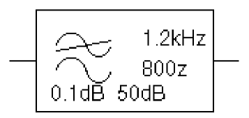
Figure 6-1 LOPASS filter part example
Assuming that the input to the filter is the voltage at net 10 and output is a voltage between nets 5 and 0, this will produce a PSpice netlist declaration like this:
ELOWPASS 5 0 CHEBYSHEV {V(10)} LP (800Hz 1.2kHz) .1dB 50dBHIPASS
|
FS |
stop band frequency |
|
FP |
pass band frequency |
|
RIPPLE |
pass band ripple in dB |
|
STOP |
stop band attenuation in dB |
The HIPASS part is characterized by two cutoff frequencies that delineate the boundaries of the filter pass band and stop band. The attenuation values, RIPPLE and STOP, define the maximum allowable attenuation in the pass band, and the minimum required attenuation in the stop band, respectively. The HIPASS part provides one input and one output.
Figure 6-2 shows an example of a HIPASS filter device. This is a high pass filter with the pass band above 1.2 kHz and the stop band below 800 Hz.
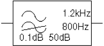
Figure 6-2 HIPASS filter part example
Again, the pass band ripple is 0.1 dB and the minimum stop band attenuation is 50 dB. This will produce a PSpice netlist declaration like this:
EHIGHPASS 5 0 CHEBYSHEV {V(10)} HP (1.2kHz 800Hz) .1dB 50dBBANDPASS
|
RIPPLE |
pass band ripple in dB |
|
STOP |
stop band attenuation in dB |
|
F0, F1, F2, F3 |
cutoff frequencies |
The BANDPASS part is characterized by four cutoff frequencies. The attenuation values, RIPPLE and STOP, define the maximum allowable attenuation in the pass band, and the minimum required attenuation in the stop band, respectively. The BANDPASS part provides one input and one output.
Figure 6-3 shows an example of a BANDPASS filter device. This is a band pass filter with the pass band between 1.2 kHz and 2 kHz, and stop bands below 800 Hz and above 3 kHz.
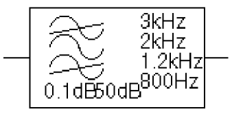
Figure 6-3 BANDPASS filter part example
The pass band ripple is 0.1 dB and the minimum stop band attenuation is 50 dB. This will produce a PSpice A/D netlist declaration like this:
EBANDPASS 5 0 CHEBYSHEV
+ {V(10)} BP (800 1.2kHz 2kHz 3kHz) .1dB 50dB
BANDREJ
|
RIPPLE |
is the pass band ripple in dB |
|
STOP |
is the stop band attenuation in dB |
|
F0, F1, F2, F3 |
are the cutoff frequencies |
The BANDREJ part is characterized by four cutoff frequencies. The attenuation values, RIPPLE and STOP, define the maximum allowable attenuation in the pass band, and the minimum required attenuation in the stop band, respectively. The BANDREJ part provides one input and one output.
Figure 6-4 shows an example of a BANDREJ filter device. This is a band reject (or “notch”) filter with the stop band between 1.2 kHz and 2 kHz, and pass bands below 800 Hz and above 3 kHz.
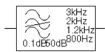
Figure 6-4 BANDREJ filter part example
The pass band ripple is 0.1 dB and the minimum stop band attenuation is 50 dB. This will produce a PSpice netlist declaration like this:
EBREJ 5 0 CHEBYSHEV {V(10)} BR (800Hz 1.2kHz 3kHz 2kHz) .1dB 50dBIntegrator and differentiator
The integrator and differentiator parts are described below.
INTEG
|
IC |
initial condition of the integrator output |
|
GAIN |
gain value |
The INTEG part implements a simple integrator. A current source/ capacitor implementation is used to provide support for setting the initial condition.
DIFFER
|
GAIN |
gain value |
The DIFFER part implements a simple differentiator. A voltage source/ capacitor implementation is used. The DIFFER part provides one input and one output.
Table look-up parts
TABLE and FTABLE parts provide a lookup table that is used to correlate an input and an output based on a set of data points. These parts are described below and on the following pages.
TABLE
|
ROWn |
is an (input, output) pair; by default, up to five triplets are allowed where n=1, 2, 3, 4, or 5 If more than five values are required, the part can be customized through the part editor. Insert additional row variables into the template using the same form as the first five, and add ROWn properties as needed to the list of properties. |
The TABLE part allows the response to be defined by a table of one to five values. Each row contains an input and a corresponding output value. Linear interpolation is performed between entries.
For values outside the table’s range, the device’s output is a constant with a value equal to the entry with the smallest (or largest) input. This characteristic can be used to impose an upper and lower limit on the output. The TABLE part provides one input and one output.
FTABLE
|
ROWn |
either an (input frequency, magnitude, phase) triplet, or an (input frequency, real part, imaginary part) triplet describing a complex value; by default, up to five triplets are allowed where n=1, 2, 3, 4, or 5 If more than five values are required, the part can be customized through the part editor. Insert additional row variables into the template using the same form as the first five, and add ROWn properties as needed to the list of properties. |
|
DELAY |
group delay increment; defaults to 0 if left blank |
|
R_I |
table type; if left blank, the frequency table is interpreted in the (input frequency, magnitude, phase) format; if defined with any value (such as YES), the table is interpreted in the (input frequency, real part, imaginary part) format |
|
MAGUNITS |
units for magnitude where the value can be DB (decibels) or MAG (raw magnitude); defaults to DB if left blank |
|
PHASEUNITS |
units for phase where the value can be DEG (degrees) or RAD (radians); defaults to DEG if left blank |
The FTABLE part is described by a table of frequency responses in either the magnitude/ phase domain (R_I= ) or complex number domain (R_I=YES). The entire table is read in and converted to magnitude in dB and phase in degrees.
Interpolation is performed between entries. Magnitude is interpolated logarithmically; phase is interpolated linearly. For frequencies outside the table’s range, 0 (zero) magnitude is used. This characteristic can be used to impose an upper and lower limit on the output.
The DELAY property increases the group delay of the frequency table by the specified amount. The delay term is particularly useful when a frequency table device generates a non-causality warning message during a transient analysis. The warning message issues a delay value that can be assigned to the part’s DELAY property for subsequent runs, without otherwise altering the table.
The output of the part depends on the analysis being done. For DC and bias point, the output is the zero frequency magnitude times the input voltage. For AC analysis, the input voltage is linearized around the bias point (similar to EVALUE and GVALUE parts, Modeling mathematical or instantaneous relationships). The output for each frequency is then the input times the gain, times the value of the table at that frequency.
For transient analysis, the voltage is evaluated at each time point. The output is then the convolution of the past values with the impulse response of the frequency response. These rules follow the standard method of using Fourier transforms. We recommend looking at one or more of the references cited in Frequency-domain device models for more information.
Example
A device, ELOFILT, is used as a frequency filter. The input to the frequency response is the voltage at net 10. The output is a voltage across nets 5 and 0. The table describes a low pass filter with a response of 1 (0 dB) for frequencies below 5 kilohertz and a response of 0.001 (-60 dB) for frequencies above 6 kilohertz. The phase lags linearly with frequency. This is the same as a constant time delay. The delay is necessary so that the impulse response is causal. That is, so that the impulse response does not have any significant components before time zero. The FTABLE part in Figure 6-5 could be used.
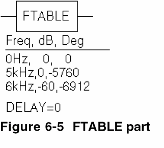
This part is characterized by the following properties:
ROW1 = 0Hz 0 0
ROW2 = 5kHz 0 -5760
ROW3 = 6kHz -60 -6912
DELAY =
R_I =
MAGUNITS =
PHASEUNITS =
Since R_I, MAGUNITS, and PHASEUNITS are undefined, each table entry is interpreted as containing frequency, magnitude value in dB, and phase values in degrees. Delay defaults to 0.
This produces a PSpice netlist declaration like this:
ELOFILT 5 0 FREQ {V(10)}
+0Hz 0 0
+5kHz 0 -5760
+6kHz -60 -6912
Since constant group delay is calculated from the values for a given table entry as:
group delay = phase / 360 / frequency
An equivalent FTABLE instance could be defined using the DELAY property. For this example, the group delay is 3.2 msec (6912 / 360 / 6k = 5760 / 360 / 6k = 3.2m). Equivalent property assignments are:
ROW1 = 0Hz 0 0
ROW2 = 5kHz 0 0
ROW3 = 6kHz -60 0
DELAY = 3.2ms
R_I =
MAGUNITS =
PHASEUNITS =
This produces a PSpice netlist declaration like this:
ELOFILT 5 0 FREQ {V(10)}
+0Hz 0 0
+5kHz 0 0
+6kHz -60 0
+DELAY=3.2ms
Laplace transform part
The LAPLACE part specifies a Laplace transform which is used to determine an output for each input value.
LAPLACE
|
NUM |
numerator of the Laplace expression |
|
DENOM |
denominator of the Laplace expression |
The LAPLACE part uses a Laplace transform description. The input to the transform is a voltage. The numerator and denominator of the Laplace transform function are specified as properties for the part.
The output of the part depends on the type of analysis being done. For DC and bias point, the output is the zero frequency gain times the value of the input. The zero frequency gain is the value of the Laplace transform with s=0. For AC analysis, the output is then the input times the gain times the value of the Laplace transform. The value of the Laplace transform at a frequency is calculated by substituting j·ω for s, where ω is 2π·frequency. For transient analysis, the output is the convolution of the input waveform with the impulse response of the transform. These rules follow the standard method of using Laplace transforms.
Example one
The input to the Laplace transform is the voltage at net 10. The output is a voltage and is applied between nets 5 and 0. For DC, the output is simply equal to the input, since the gain at s=0 is 1. The transform, 1/(1+.001·s), describes a simple, lossy integrator with a time constant of 1 millisecond. This can be implemented with an RC pair that has a time constant of 1 millisecond.
For AC analysis, the gain is found by substituting j·ω for s. This gives a flat response out to a corner frequency of 1000/(2π) = 159 hertz and a roll-off of 6 dB per octave after 159 Hz. There is also a phase shift centered around 159 Hz. In other words, the gain has both a real and an imaginary component. For transient analysis, the output is the convolution of the input waveform with the impulse response of 1/(1+.001·s). The impulse response is a decaying exponential with a time constant of 1 millisecond. This means that the output is the “lossy integral” of the input, where the loss has a time constant of 1 millisecond. The LAPLACE part shown in Figure 6-6 could be used for this purpose.
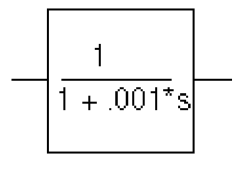
Figure 6-6 LAPLACE part
The transfer function is the Laplace transform (1/[1+.001*s]). This LAPLACE part is characterized by the following properties:
NUM = 1
DENOM = 1 + .001*s
The gain and phase characteristics are shown in Figure 6-7.
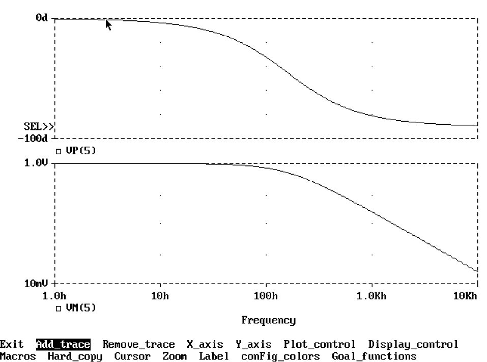
Figure 6-7 Viewing gain and phase characteristics of a lossy integrator.
This produces a PSpice netlist declaration like this:
ERC 5 0 LAPLACE {V(10)} = {1/(1+.001*s)}Example two
The input is V(10). The output is a current applied between nets 5 and 0. The Laplace transform describes a lossy transmission line. R, L, and C are the resistance, inductance, and capacitance of the line per unit length.
If R is small, the characteristic impedance of such a line is Z = ((R + j·ω·L)/(j·ω·C))1/2, the delay per unit length is (L C)1/2, and the loss in dB per unit length is 23·R/Z. This could be represented by the device in Figure 6-8.
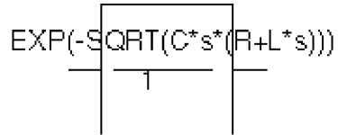
Figure 6-8 LAPLACE part
The parameters R, L, and C can be defined in a .PARAM statement contained in a model file. (Refer to the PSpice A/D Reference Guide for more information about using .PARAM statements.) More useful, however, is for R, L, and C to be arguments passed into a subcircuit. This part has the following characteristics:
NUM = EXP(-SQRT(C*s*(R+L*s)))
DENOM = 1
This produces a PSpice netlist declaration like this:
GLOSSY 5 0 LAPLACE {V(10)} = {exp(-sqrt(C*s*(R + L*s)))}The Laplace transform parts are, however, an inefficient way, in both computer time and memory, to implement a delay. For ideal delays we recommend using the transmission line part instead.
Math functions
The ABM math function parts are shown in Table 6-2. Math function parts are based on the PSpice “E” device type. Each provides one or more inputs, and a mathematical function which is applied to the input. The result is output on the output net.
| For this device... | Output is the... |
|---|---|
|
ABS |
absolute value of the input |
|
SQRT |
square root of the input |
|
PWR |
result of raising the absolute value of the input to the power specified by EXP |
|
PWRS |
result of raising the (signed) input value to the power specified by EXP |
|
LOG |
LOG of the input |
|
LOG10 |
LOG10 of the input |
|
EXP |
result of e raised to the power specified by the input value (exwhere x is the input) |
|
SIN |
sin of the input (where the input is in radians) |
|
COS |
cos of the input (where the input is in radians) |
|
TAN |
tan of the input (where the input is in radians) |
|
ATAN, |
tan-1of the input (where the output is in radians) |
ABM expression parts
The expression parts are shown in Table 6-3. These parts can be customized to perform a variety of functions depending on your requirements. Each of these parts has a set of four expression building block properties of the form:
EXPn
where n = 1, 2, 3, or 4.
During netlist generation, the complete expression is formed by concatenating the building block expressions in numeric order, thus defining the transfer function. Hence, the first expression fragment should be assigned to the EXP1 property, the second fragment to EXP2, and so on.
Expression properties can be defined using a combination of arithmetic operators and input designators. You may use any of the standard PSpice arithmetic operators (see Table 3-3) within an expression statement. You may also use the EXPn properties as variables to represent nets or constants.
| Part | Inputs | Output |
|---|---|---|
|
ABM |
none |
V |
|
ABM1 |
1 |
V |
|
ABM2 |
2 |
V |
|
ABM3 |
3 |
V |
|
ABM/I |
none |
I |
|
ABM1/I |
1 |
I |
|
ABM2/I |
2 |
I |
|
ABM3/I |
3 |
I |
The following examples illustrate a variety of ABM expression part applications.
Example one
Suppose you want to set an output voltage on net 4 to 5 volts times the square root of the voltage between nets 3 and 2. You could use an ABM2 part (which takes two inputs and provides a voltage output) to define a part like the one shown in Figure 6-9.
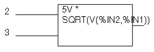
Figure 6-9 ABM expression part example one.
In this example of an ABM device, the output voltage is set to 5 volts times the square root of the voltage between net 3 and net 2. The property settings for this part are as follows:
EXP1 = 5V *
EXP2 = SQRT(V(%IN2,%IN1))
This will produce a PSpice netlist declaration like this:
ESQROOT 4 0 VALUE = {5V*SQRT(V(3,2))}Example two
GPSK is an oscillator for a PSK (Phase Shift Keyed) modulator. Current is pumped from net 11 through the source to net 6. Its value is a sine wave with an amplitude of 15 mA and a frequency of 10 kHz. The voltage at net 3 can shift the phase of GPSK by 1 radian/ volt. Note the use of the TIME parameter in the EXP2 expression. This is the PSpice A/D internal sweep variable used in transient analysis. For any analysis other than transient, TIME = 0. This could be represented with an ABM1/I part (single input, current output) like the one shown in Figure 6-10.
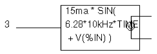
Figure 6-10 ABM expression part example two.
This part is characterized by the following properties:
EXP1 = 15ma * SIN(
EXP2 = 6.28*10kHz*TIME
EXP3 = + V(%IN))
This produces a PSpice netlist declaration like this:
GPSK 11 6 VALUE = {15MA*SIN(6.28*10kHz*TIME+V(3))}Example three
A device, EPWR, computes the instantaneous power by multiplying the voltage across nets 5 and 4 by the current through VSENSE. Sources are controlled by expressions which may contain voltages or currents or both. The ABM2 part (two inputs, voltage output) in Figure 6-11 could represent this.
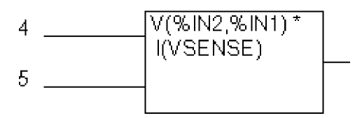
Figure 6-11 ABM expression part example three.
This part is characterized by the following properties:
EXP1 = V(%IN2,%IN1) *
EXP2 = I(VSENSE)
This produces a PSpice netlist declaration like this:
EPWR 3 0 VALUE = {V(5,4)*I(VSENSE)}Example four
The output of a component, GRATIO, is a current whose value (in amps) is equal to the ratio of the voltages at nets 13 and 2. If V(2) = 0, the output depends upon V(13) as follows:
if V(13) = 0, output = 0 if V(13) > 0, output = MAXREAL if V(13) < 0, output = -MAXREAL
where MAXREAL is a PSpice internal constant representing a very large number (on the order of 1e30). In general, the result of evaluating an expression is limited to MAXREAL. This is modeled with an ABM2/I (two input, current output) part like this one in 6-12.
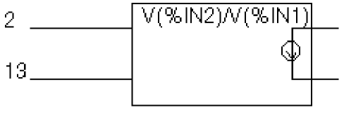
Figure 6-12 ABM expression part example four.
This part is characterized by the following properties:
EXP1 = V(%IN2)/V(%IN1)
Note that output of GRATIO can be used as part of the controlling function. This produces a PSpice netlist declaration like this:
GRATIO 2 3 VALUE = {V(13)/V(2)} An instantaneous device example: modeling a triode
This section provides an example of using various ABM parts to model a triode vacuum tube. The schematic of the triode subcircuit is shown in Figure 6-13.
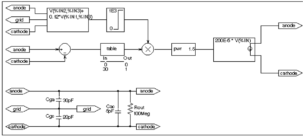
Figure 6-13 Triode circuit.
Assumptions: In its main operating region, the triode’s current is proportional to the 3/2 power of a linear combination of the grid and anode voltages:
ianode = k0*(vg + k1*va)1.5
For a typical triode, k0 = 200e-6 and k1 = 0.12.
Looking at the upper left-hand portion of the schematic, notice the a general-purpose ABM part used to take the input voltages from anode, grid, and cathode. Assume the following associations:
- V(anode) is associated with V(%IN1)
- V(grid) is associated with V(%IN2)
- V(cathode) is associated with V(%IN3)
The expression property EXP1 then represents V(grid, cathode) and the expression property EXP2 represents 0.12[V(anode, cathode)]. When the template substitution is performed, the resulting VALUE is equivalent to the following:
V = V(grid, cathode) + 0.12*V(anode, cathode)
The part would be defined with the following characteristics:
EXP1 = V(%IN2,%IN3)+
EXP2 = 0.12*V(%IN1,%IN3)
This works for the main operating region but does not model the case in which the current stays 0 when combined grid and anode voltages go negative. We can accommodate that situation as follows by adding the LIMIT part with the following characteristics:
HI = 1E3
LO = 0
This part instance, LIMIT1, converts all negative values of vg+.12*va to 0 and leaves all positive values (up to 1 kV) alone. For a more realistic model, we could have used TABLE to correctly model how the tube turns off at 0 or at small negative grid voltages.
We also need to make sure that the current becomes zero when the anode alone goes negative. To do this, we can use a DIFF device, (immediately below the ABM3 device) to monitor the difference between V(anode) and V(cathode), and output the difference to the TABLE part. The table translates all values at or below zero to zero, and all values greater than or equal to 30 to one. All values between 0 and 30 are linearly interpolated. The properties for the TABLE part are as follows:
ROW1 = 0 0
ROW2 = 30 1
The TABLE part is a simple one, and ensures that only a zero value is output to the multiplier for negative anode voltages.
The output from the TABLE part and the LIMIT part are combined at the MULT multiplier part. The output of the MULT part is the product of the two input voltages. This value is then raised to the 3/2 or 1.5 power using the PWR part. The exponential property of the PWR part is defined as follows:
EXP = 1.5
The last major component is an ABM expression component to take an input voltage and convert it into a current. The relevant ABM1/I part property looks like this:
EXP1 = 200E-6 * V(%IN)
A final step in the model is to add device parasitics. For example, a resistor can be used to give a finite output impedance. Capacitances between the grid, cathode, and anode are also needed. The lower part of the schematic in Figure 6-13 shows a possible method for incorporating these effects. To complete the example, one could add a circuit which produces the family of I-V curves (shown in Figure 6-14).
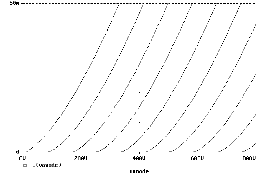
Figure 6-14 Triode subcircuit producing a family of I-V curves.
PSpice-equivalent parts
PSpice-equivalent parts respond to a differential input and have double-ended output. These parts reflect the structure of PSpice E and G devices, thus having two pins for each controlling input and the output in the part. Table 6-4 summarizes the PSpice-equivalent parts available in the part library.
| Category | Part | Description | Properties |
|---|---|---|---|
|
Mathematical expression |
EVALUE |
general purpose |
EXPR |
|
GVALUE |
|||
|
ESUM |
special purpose |
(none) |
|
|
GSUM |
|||
|
EMULT |
|||
|
GMULT |
|||
|
Table look-up |
ETABLE |
general purpose |
EXPR |
|
GTABLE |
TABLE |
||
|
Frequency table look-up |
EFREQ |
general purpose |
EXPR |
|
GFREQ |
TABLE |
||
|
Laplace transform |
ELAPLACE |
general purpose |
EXPR |
|
GLAPLACE |
XFORM |
PSpice-equivalent ABM parts can be classified as either E or G device types. The E part type provides a voltage output, and the G device type provides a current output.
The device’s transfer function can contain any mixture of voltages and currents as inputs. Hence, there is no longer a division between voltage-controlled and current-controlled parts. Rather the part type is dictated only by the output requirements. If a voltage output is required, use an E part type. If a current output is necessary, use a G part type.
Each E or G part type in the ABM.OLB part file is defined by a template that provides the specifics of the transfer function. Other properties in the model definition can be edited to customize the transfer function. By default, the template cannot be modified directly choosing Properties from the Edit menu in Capture. Rather, the values for other properties (such as the expressions used in the template) are usually edited, then these values are substituted into the template. However, the part editor can be used to modify the template or designate the template as modifiable from within Capture. This way, custom parts can be created for special-purpose application.
Implementation of PSpice-equivalent parts
Although you generally use Capture to place and specify PSpice-equivalent ABM parts, it is useful to know the PSpice command syntax for “E” and “G” devices. This is especially true when creating custom ABM parts since part templates must adhere to PSpice syntax.
The general forms for PSpice “E” and “G” extensions are:
E <name> <connecting nodes> <ABM keyword> <ABM function>
G <name> <connecting nodes> <ABM keyword> <ABM function>
where
|
<name> |
is the device name appended to the E or G device type character |
|
<connecting nodes> |
specifies the <(+ node name, - node name)> pair between which the device is connected |
|
<ABM keyword> |
specifies the form of the transfer function to be used, as one of: VALUE arithmetic expression |
|
<ABM function> |
specifies the transfer function as a formula or lookup table as required by the specified <ABM keyword> |
Refer to the PSpice A/D Reference Guide for detailed information.
Modeling mathematical or instantaneous relationships
The instantaneous models (using VALUE and TABLE extensions to PSpice “E” and “G” devices in the part templates) enforce a direct response to the input at each moment in time. For example, the output might be equal to the square root of the input at every point in time. Such a device has no memory, or, a flat frequency response. These techniques can be used to model both linear and nonlinear responses.
EVALUE and GVALUE parts
The EVALUE and GVALUE parts allow an instantaneous transfer function to be written as a mathematical expression in standard notation. These parts take the input signal, perform the function specified by the EXPR property on the signal, and output the result on the output pins.
In controlled sources, EXPR may contain constants and parameters as well as voltages, currents, or time. Voltages may be either the voltage at a net, such as V(5), or the voltage across two nets, such as V(4,5). Currents must be the current through a voltage source (V device), for example, I(VSENSE). Voltage sources with a value of 0 are handy for sensing current for use in these expressions.
Functions may be used in expressions, along with arithmetic operators (+, -, *, and /) and parentheses. Available built-in functions are summarized in Table 3-4.
The EVALUE and GVALUE parts are defined, in part, by the following properties (default values are shown):
EVALUE
EXPR V(%IN+, %IN-)
GVALUE
EXPR V(%IN+, %IN-)
Sources are controlled by expressions which may contain voltages, currents, or both. The following examples illustrate customized EVALUE and GVALUE parts.
Example 1
In the example of an EVALUE device shown in Figure 6-15, the output voltage is set to 5 volts times the square root of the voltage between pins %IN+ and %IN-.
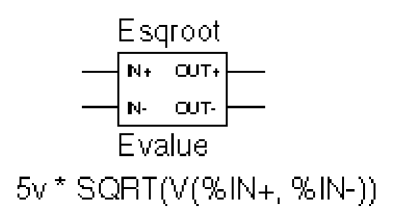
Figure 6-15 EVALUE part example.
The property settings for this device are as follows:
EXPR = 5v * SQRT(V(%IN+,%IN-))
Example 2
Consider the device in Figure 6-16. This device could be used as an oscillator for a PSK (Phase Shift Keyed) modulator.
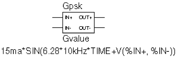
Figure 6-16 GVALUE part example.
A current through a source is a sine wave with an amplitude of 15 mA and a frequency of 10 kHz. The voltage at the input pin can shift the phase by 1 radian/volt. Note the use of the TIME parameter in this expression. This is the PSpice internal sweep variable used in transient analyses. For any analysis other than transient, TIME = 0. The relevant property settings for this device are shown below:
EXPR = 15ma*SIN(6.28*10kHz*TIME+V(%IN+,%IN-))
EMULT, GMULT, ESUM, and GSUM
The EMULT and GMULT parts provide output which is based on the product of two input sources. The ESUM and GSUM parts provide output which is based on the sum of two input sources. The complete transfer function may also include other mathematical expressions.
Example 1
Consider the device in Figure 6-17. This device computes the instantaneous power through resistor VSENSE by multiplying the current through VSENSE (converted to voltage by H1) by the voltage across VSENSE.
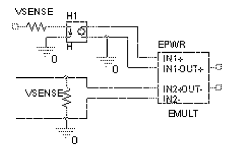
Figure 6-17 EMULT part example.
This device’s behavior is built-in to the PSPICETEMPLATE property as follows (appears on one line):
TEMPLATE=E^@REFDES %OUT+ %OUT- VALUE {V(%IN1+,%IN1-)
 *V(%IN2+,%IN2-)}
You can use the part editor to change the characteristics of the template to accommodate additional mathematical functions, or to change the nature of the transfer function itself. For example, you may want to create a voltage divider, rather than a multiplier. This is illustrated in the following example.
Example 2
Consider the device in Figure 6-18.
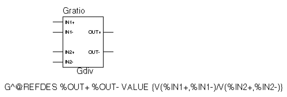
Figure 6-18 GMULT part example.
With this device, the output is a current is equal to the ratio of the voltages at input pins 1 and input pins 2. If V(%IN2+, %IN2-) = 0, the output depends upon V(%IN1+, %IN1-) as follows:
if V(%IN1+, %IN1-) = 0, output = 0 if V(%IN1+, %IN1-) > 0, output = MAXREAL if V(%IN1+, %IN1-) < 0, output = -MAXREAL
where MAXREAL is a PSpice internal constant representing a very large number (on the order of 1e30). In general, the result of evaluating an expression is limited to MAXREAL. Note that the output of the part can also be used as part of the controlling function.
To create this device, you would first make a new part, GDIV, based on the GMULT part. Edit the GDIV template to divide the two input values rather than multiply them.
Lookup tables (ETABLE and GTABLE)
The ETABLE and GTABLE parts use a transfer function described by a table. These device models are well suited for use with measured data.
The ETABLE and GTABLE parts are defined in part by the following properties (default values are shown):
ETABLE
TABLE (-15, -15), (15,15) EXPR V(%IN+, %IN-)
GTABLE
TABLE (-15, -15), (15,15) EXPR V(%IN+, %IN-)
First, EXPR is evaluated, and that value is used to look up an entry in the table. EXPR is a function of the input (current or voltage) and follows the same rules as for VALUE expressions.
The table consists of pairs of values, the first of which is an input, and the second of which is the corresponding output. Linear interpolation is performed between entries. For values of EXPR outside the table’s range, the device’s output is a constant with a value equal to the entry with the smallest (or largest) input. This characteristic can be used to impose an upper and lower limit on the output.
An example of a table declaration (using the TABLE property) would be the following:
TABLE =
+ (0, 0) (.02, 2.690E-03) (.04, 4.102E-03) (.06, 4.621E-03)
+ (.08, 4.460E-03) (.10, 3.860E-03) (.12, 3.079E-03) (.14,
+ 2.327E-03)
+ (.16, 1.726E-03) (.18, 1.308E-03) (.20, 1.042E-03) (.22,
+ 8.734E-04)
+ (.24, 7.544E-04) (.26, 6.566E-04) (.28, 5.718E-04) (.30,
+ 5.013E-04)
+ (.32, 4.464E-04) (.34, 4.053E-04) (.36, 3.781E-04) (.38,
+ 3.744E-04)
+ (.40, 4.127E-04) (.42, 5.053E-04) (.44, 6.380E-04) (.46,
+ 7.935E-04)
+ (.48, 1.139E-03) (.50, 2.605E-03) (.52, 8.259E-03) (.54,
+ 2.609E-02)
+ (.56, 7.418E-02) (.58, 1.895E-01) (.60, 4.426E-01)
Frequency-domain device models
Frequency-domain models (ELAPLACE, GLAPLACE, EFREQ, and GFREQ) are characterized by output that depends on the current input as well as the input history. The relationship is therefore non-instantaneous. For example, the output may be equal to the integral of the input over time. In other words, the response depends upon frequency.
During AC analysis, the frequency response determines the complex gain at each frequency. During DC analysis and bias point calculation, the gain is the zero-frequency response. During transient analysis, the output of the device is the convolution of the input and the impulse response of the device.
Moving back and forth between the time and frequency-domains can cause surprising results. Often the results are quite different than what one would intuitively expect. For this reason, we strongly recommend familiarity with a reference on Fourier and Laplace transforms. A good one is:
- R. Bracewell, The Fourier Transform and Its Applications, McGraw-Hill, Revised Second Edition (1986)
We also recommend familiarity with the use of transforms in analyzing linear systems. Some references on this subject:
- W. H. Chen, The Analysis of Linear Systems, McGraw-Hill (1962)
- J. A. Aseltine, Transform Method in Linear System Analysis, McGraw-Hill (1958)
Laplace transforms (LAPLACE)
The ELAPLACE and GLAPLACE parts allow a transfer function to be described by a Laplace transform function. The ELAPLACE and GLAPLACE parts are defined, in part, by the following properties (default values are shown):
ELAPLACE
EXPR V(%IN+, %IN-) XFORM 1/s
GLAPLACE
EXPR V(%IN+, %IN-) XFORM 1/s
The LAPLACE parts use a Laplace transform description. The input to the transform is the value of EXPR, where EXPR follows the same rules as for VALUE expressions (see EVALUE and GVALUE parts). XFORM is an expression in the Laplace variable, s. It follows the rules for standard expressions as described for VALUE expressions with the addition of the s variable.
The output of the device depends on the type of analysis being done. For DC and bias point, the output is simply the zero frequency gain times the value of EXPR. The zero frequency gain is the value of XFORM with s = 0. For AC analysis, EXPR is linearized around the bias point (similar to the VALUE parts). The output is then the input times the gain of EXPR times the value of XFORM. The value of XFORM at a frequency is calculated by substituting j·w for s, where w is 2p·frequency. For transient analysis, the value of EXPR is evaluated at each time point. The output is then the convolution of the past values of EXPR with the impulse response of XFORM. These rules follow the standard method of using Laplace transforms. We recommend looking at one or more of the references cited in Frequency-domain device models for more information.
Example
The input to the Laplace transform is the voltage across the input pins, or V(%IN+, %IN-). The EXPR property may be edited to include constants or functions, as with other parts. The transform, 1/(1+.001·s), describes a simple, lossy integrator with a time constant of 1 millisecond. This can be implemented with an RC pair that has a time constant of 1 millisecond.
Using the part editor, you would define the XFORM and EXPR properties as follows:
XFORM = 1/(1+.001*s)
EXPR = V(%IN+, %IN-)
The default template remains (appears on one line):
TEMPLATE= E^@REFDES %OUT+ %OUT- LAPLACE {@EXPR}= (@XFORM)After netlist substitution of the template, the resulting transfer function would become:
V(%OUT+, %OUT-) = LAPLACE {V(%IN+, %IN-)}= (1/1+.001*s))The output is a voltage and is applied between pins %OUT+ and %OUT-. For DC, the output is simply equal to the input, since the gain at s = 0 is 1.
For AC analysis, the gain is found by substituting j·ω for s. This gives a flat response out to a corner frequency of 1000/(2π) = 159 Hz and a roll-off of 6 dB per octave after 159 Hz. There is also a phase shift centered around 159 Hz. In other words, the gain has both a real and an imaginary component. The gain and phase characteristic is the same as that shown for the equivalent control system part example using the LAPLACE part (see Figure 6-7).
For transient analysis, the output is the convolution of the input waveform with the impulse response of 1/(1+.001·s). The impulse response is a decaying exponential with a time constant of 1 millisecond. This means that the output is the “lossy integral” of the input, where the loss has a time constant of 1 millisecond.
This will produce a PSpice A/D netlist declaration similar to:
ERC 5 0 LAPLACE {V(10)} = {1/(1+.001*s)}Frequency response tables (EFREQ and GFREQ)
The EFREQ and GFREQ parts are described by a table of frequency responses in either the magnitude/phase domain or complex number domain. The entire table is read in and converted to magnitude in dB and phase in degrees. Interpolation is performed between entries. Phase is interpolated linearly; magnitude is interpolated logarithmically. For frequencies outside the table’s range, 0 (zero) magnitude is used.
EFREQ and GFREQ properties are defined as follows:
|
EXPR |
value used for table lookup; defaults to V(%IN+, %IN-) if left blank. |
|
TABLE |
series of either (input frequency, magnitude, phase) triplets, or (input frequency, real part, imaginary part) triplets describing a complex value; defaults to (0,0,0) (1Meg,-10,90) if left blank. |
|
DELAY |
group delay increment; defaults to 0 if left blank. |
|
R_I |
table type; if left blank, the frequency table is interpreted in the (input frequency, magnitude, phase) format; if defined with any value (such as YES), the table is interpreted in the (input frequency, real part, imaginary part) format. |
|
MAGUNITS |
units for magnitude where the value can be DB (decibels) or MAG (raw magnitude); defaults to DB if left blank. |
|
PHASEUNITS |
units for phase where the value can be DEG (degrees) or RAD (radians); defaults to DEG if left blank. |
The DELAY property increases the group delay of the frequency table by the specified amount. The delay term is particularly useful when an EFREQ or GFREQ device generates a non-causality warning message during a transient analysis. The warning message issues a delay value that can be assigned to the part’s DELAY property for subsequent runs, without otherwise altering the table.
The output of the device depends on the analysis being done. For DC and bias point, the output is simply the zero frequency magnitude times the value of EXPR. For AC analysis, EXPR is linearized around the bias point (similar to EVALUE and GVALUE parts). The output for each frequency is then the input times the gain of EXPR times the value of the table at that frequency. For transient analysis, the value of EXPR is evaluated at each time point. The output is then the convolution of the past values of EXPR with the impulse response of the frequency response. These rules follow the standard method of using Fourier transforms. We recommend looking at one or more of the references cited in Frequency-domain device models for more information.
Figure 6-19 shows an EFREQ device used as a low pass filter.
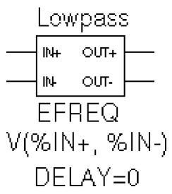
Figure 6-19 EFREQ part example.
The input to the frequency response is the voltage across the input pins. The table describes a low pass filter with a response of 1 (0 dB) for frequencies below 5 kilohertz and a response of .001 (-60 dB) for frequencies above 6 kilohertz. The output is a voltage across the output pins.
This part is defined by the following properties:
TABLE = (0, 0, 0) (5kHz, 0, -5760) (6kHz, -60, -6912)
DELAY =
R_I =
MAGUNITS =
PHASEUNITS =
Since R_I, MAGUNITS, and PHASEUNITS are undefined, each table entry is interpreted as containing frequency, magnitude value in dB, and phase values in degrees. Delay defaults to 0.
The phase lags linearly with frequency meaning that this table exhibits a constant time (group) delay. The delay is necessary so that the impulse response is causal. That is, so that the impulse response does not have any significant components before time zero.
The constant group delay is calculated from the values for a given table entry as follows:
group delay = phase / 360 / frequency
For this example, the group delay is 3.2 msec
(6912 / 360 / 6k = 5760 / 360 / 6k = 3.2m). An alternative specification for this table could be:
TABLE = (0, 0, 0) (5kHz, 0, 0) (6kHz, -60, 0)
DELAY = 3.2ms
R_I =
MAGUNITS =
PHASEUNITS =
This produces a PSpice netlist declaration like this:
ELOWPASS 5 0 FREQ {V(10)} = (0,0,0) (5kHz,0,0) (6kHz-60,0)
+ DELAY = 3.2ms
Cautions and recommendations for simulation and analysis
Instantaneous device modeling
During AC analysis, nonlinear transfer functions are handled the same way as other nonlinear parts: each function is linearized around the bias point and the resulting small-signal equivalent is used.
Consider the voltage multiplier (mixer) shown in Figure 6-20.
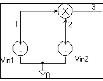
Figure 6-20 Voltage multiplier circuit (mixer).
This circuit has the following characteristics:
Vin1: DC=0v AC=1v Vin2: DC=0v AC=1v
where the output on net 3 is V(1)*V(2).
During AC analysis, V(3) = 0 due to the 0 volts bias point voltage on nets 1, 2, and 3. The small-signal equivalent therefore has 0 gain (the derivative of V(1)*V(2) with respect to both V(1) and V(2) is 0 when V(1)=V(2)=0). So, the output of the mixer during AC analysis will be 0 regardless of the AC values of V(1) and V(2).
Another way of looking at this is that a mixer is a nonlinear device and AC analysis is a linear analysis. The output of the mixer has 0 amplitude at the fundamental. (Output is nonzero at DC and twice the input frequency, but these are not included in a linear analysis.)
If you need to analyze nonlinear functions, such as a mixer, use transient analysis. Transient analysis solves the full, nonlinear circuit equations. It also allows you to use input waveforms with different frequencies (for example, VIN1 could be 90 MHz and VIN2 could be 89.8 MHz). AC analysis does not have this flexibility, but in return it uses much less computer time.
Frequency-domain parts
Some caution is in order when moving between frequency and time domains. This section discusses several points that are involved in the implementation of frequency-domain parts. These discussions all involve the transient analysis, since both the DC and AC analyses are straightforward.
The first point is that there are limits on the maximum values and on the resolution of both time and frequency. These are related: the frequency resolution is the inverse of the maximum time and vice versa. The maximum time is the length of the transient analysis, TSTOP. Therefore, the frequency resolution is 1/TSTOP.
Laplace transforms
For Laplace transforms, PSpice A/D starts off with initial bounds on the frequency resolution and the maximum frequency determined by the transient analysis parameters as follows. The frequency resolution is initially set below the theoretical limit to (.25/TSTOP) and is then made as large as possible without inducing sampling errors. The maximum frequency has an initial upper bound of (1/(RELTOL*TMAX)), where TMAX is the transient analysis Step Ceiling value, and RELTOL is the relative accuracy of all calculated voltages and currents. If a Step Ceiling value is not specified, PSpice A/D uses the Transient Analysis Print Step, TSTEP, instead.
PSpice A/D then attempts to reduce the maximum frequency by searching for the frequency at which the response has fallen to RELTOL times the maximum response. For instance, for the transform:
1/(1+s)
the maximum response, 1.0, is at s = j·ω = 0 (DC). The cutoff frequency used when RELTOL=.001, is approximately 1000/(2π) = 159 Hz. At 159 Hz, the response is down to .001 (down by 60 db). Since some transforms do not have such a limit, there is also a limit of 10/RELTOL times the frequency resolution, or 10/(RELTOL·TSTOP). For example, consider the transform:
e-0.001·s
This is an ideal delay of 1 millisecond and has no frequency cutoff. If TSTOP = 10 milliseconds and RELTOL=.001, then PSpice A/D imposes a frequency cutoff of 10 MHz. Since the time resolution is the inverse of the maximum frequency, this is equivalent to saying that the delay cannot resolve changes in the input at a rate faster than .1 microseconds. In general, the time resolution will be limited to RELTOL·TSTOP/10.
A final computational consideration for Laplace parts is that the impulse response is determined by means of an FFT on the Laplace expression. The FFT is limited to 8192 points to keep it tractable, and this places an additional limit on the maximum frequency, which may not be greater than 8192 times the frequency resolution.
If your circuit contains many Laplace parts which can be combined into a more complex single device, it is generally preferable to do this. This saves computation and memory since there are fewer impulse responses. It also reduces the number of opportunities for numerical artifacts that might reduce the accuracy of your transient analyses.
Laplace transforms can contain poles in the left half-plane. Such poles will cause an impulse response that increases with time instead of decaying. Since the transient analysis is always for a finite time span, PSpice A/D does not have a problem calculating the transient (or DC) response. However, such poles will make the actual device oscillate.
Non-causality and Laplace transforms
PSpice A/D applies an inverse FFT to the Laplace expression to obtain an impulse response, and then convolves the impulse response with the dependent source input to obtain the output. Some common impulse responses are inherently non-causal. This means that the convolution must be applied to both past and future samples of the input in order to properly represent the inverse of the Laplace expression.
For example, the expression {S} corresponds to differentiation in the time domain. The impulse response for {S} is an impulse pair separated by an infinitesimal distance in time. The impulses have opposite signs, and are situated one in the infinitesimal past, the other in the infinitesimal future. In other words, convolution with this corresponds to applying a finite-divided difference in the time domain.
The problem with this for PSpice A/D is that the simulator only has the present and past values of the simulated input, so it can only apply half of the impulse pair during convolution. This will obviously not result in time-domain differentiation. PSpice A/D can detect, but not fix this condition, and issues a non-causality warning message when it occurs. The message tells what percentage of the impulse response is non-causal, and how much delay would need to be added to slide the non-causal part into a causal region. {S} is theoretically 50% non-causal. Non-causality on the order of 1% or less is usually not critical to the simulation results.
You can delay {S} to keep it causal, but the separation between the impulses is infinitesimal. This means that a very small time step is needed. For this reason, it is usually better to use a macromodel to implement differentiation.
Here are some guidelines:
- In the case of a Laplace device (ELAPLACE), multiply the Laplace expression by e to the (-s
- In the case of a frequency table (EFREQ or GFREQ), do either of the following:
- Specify the table with
DELAY=<the suggested delay>. - Compute the delay by adding a phase shift.
- Specify the table with
Chebyshev filters
All of the considerations given above for Laplace parts also apply to Chebyshev filter parts. However, PSpice A/D also attempts to deal directly with inaccuracies due to sampling by applying Nyquist criteria based on the highest filter cutoff frequency. This is done by checking the value of TMAX. If TMAX is not specified it is assigned a value, or if it is specified, it may be reduced.
For low pass and band pass filters, TMAX is set to (0.5/FS), where FS is the stop band cutoff in the case of a low pass filter, or the upper stop band cutoff in the case of a band pass filter.
For high pass and band reject filters, there is no clear way to apply the Nyquist criterion directly, so an additional factor of two is thrown in as a safety margin. Thus, TMAX is set to (0.25/FP), where FP is the pass band cutoff for the high pass case or the upper pass band cutoff for the band reject case. It may be necessary to set TMAX to something smaller if the filter input has significant frequency content above these limits.
Frequency tables
For frequency response tables, the maximum frequency is twice the highest value. It will be reduced to 10/(RELTOL⋅TSTOP) or 8192 times the frequency resolution if either value is smaller.
The frequency resolution for frequency response tables is taken to be either the smallest frequency increment in the table or the fastest rate of phase change, whichever is least. PSpice A/D then checks to see if it can be loosened without inducing sampling errors.
Trading off computer resources for accuracy
There is a significant trade-off between accuracy and computation time for parts modeled in the frequency domain. The amount of computer time and memory scale approximately inversely to RELTOL. Therefore, if you can use RELTOL=.01 instead of the default .001, you will be ahead. However, this will not adversely affect the impulse response. You may also wish to vary TMAX and TSTOP, since these also come into play.
Since the trade-off issues are fairly complex, it is advisable to first simulate a small test circuit containing only the frequency-domain device, and then after proper validation, proceed to incorporate it in your larger design. The PSpice A/D defaults will be appropriate most of the time if accuracy is your main concern, but it is still worth checking.
Basic controlled sources
As with basic SPICE, PSpice A/D has basic controlled sources derived from the standard SPICE E, F, G, and H devices. Table 6-5 summarizes the linear controlled source types provided in the standard part library.
| Device type | Part name |
|---|---|
|
Controlled Voltage Source (PSpice A/D E device) |
E |
|
Current-Controlled Current Source (PSpice A/D F device) |
F |
|
Controlled Current Source (PSpice A/D G device) |
G |
|
Current-Controlled Voltage Source (PSpice A/D H device) |
H |
Creating custom ABM parts
Create a custom part when you need a controlled source that is not provided in the special purpose set or that is more elaborate than you can build with the general purpose parts (with multiple controlling inputs, for example). Refer to your OrCAD X Capture User Guide for a description of how to create a custom part.
The transfer function can be built into the part two different ways:
- directly in the PSPICETEMPLATE definition.
- by defining the part’s EXPR and related properties (if any).
View the next document: 07 - Digital Models for Circuit Simulation
If you have any questions or comments about the OrCAD X platform, click on the link below.
Contact Us