14 - Digital Simulation
What is digital simulation?
Digital simulation is the analysis of logic and timing behavior of digital devices over time. PSpice A/D simulates this behavior during transient analysis. When computing the bias point, PSpice A/D considers the digital devices in addition to any analog devices in the circuit.
PSpice A/D performs detailed timing analysis subject to the constraints specified for the devices. For example, flip-flops perform setup checks on the incoming clock and data signals. PSpice A/D reports any timing violations or hazards as messages written to the simulation output file and the waveform data file. See Tracking timing violations and hazards for information about persistent hazards, and for descriptions of the warning messages.
Steps for simulating digital circuits
There are six steps in the development and simulation of digital circuits:
- Drawing the design.
For more information on drawing designs see your OrCAD X Capture User Guide. Steps 2 through 6 of this process are covered in this chapter. - Defining the stimuli.
- Setting the simulation time.
- Adjusting the simulation parameters.
- Starting the simulation.
- Analyzing the results.
Concepts you need to understand
States
When the circuit is in operation, digital nodes take on values or output states shown in Table 14-1. Each digital state has a strength component as well. Strengths are described in the next section.
| This state... | Means this... |
|---|---|
|
0 |
Low, false, no, off |
|
1 |
High, true, yes, on |
|
R |
Rising (changes from 0 to 1 sometime during the R interval) |
|
F |
Falling (changes from 1 to 0 sometime during the F interval) |
|
X |
Unknown: may be high, low, intermediate, or unstable |
|
Z |
High impedance: may be high, low, intermediate, or unstable |
Strengths
When a digital node is driven by more than one device, PSpice A/D determines the correct level of the node. Each output has a strength value, and PSpice A/D compares the strengths of the outputs driving the node. The strongest driver determines the resulting level of the node. If outputs of the same strength but different levels drive a node, the node’s level becomes X.
PSpice A/D supports 64 strengths. The lowest (weakest) strength is called Z. The highest (strongest) strength is called the forcing strength. The Z strength (called high impedance) is typically output by disabled tristate gates or open-collector output devices. PSpice A/D reports any nodes of Z strength (at any level) as Z, and reports all other nodes by the designations shown in Digital states.
Defining a digital stimulus
A digital stimulus defines input to the digital portions of your circuit, playing a role similar to that played by the independent voltage and current sources for the analog portion of your circuit.
The following table summarizes the digital stimuli provided in the part libraries.
| If you want to specify the input signal by... | Then use this part... | For this type of digital input... |
|---|---|---|
|
Using the Stimulus Editor |
DIGSTIMn |
signal or bus stimulus |
|
Defining part properties |
DIGCLOCK |
clock signal |
|
STIM1 |
one-bit stimulus |
|
|
STIM4 |
four-bit stimulus |
|
|
STIM8 |
eight-bit stimulus |
|
|
STIM16 |
sixteen-bit stimulus |
|
|
FILESTIM1 |
one-bit file-based stimulus |
|
|
FILESTIM2 |
two-bit file-based stimulus |
|
|
FILESTIM4 |
four-bit file-based stimulus |
|
|
FILESTIM8 |
eight-bit file-based stimulus |
|
|
FILESTIM16 |
sixteen-bit file-based stimulus |
|
|
FILESTIM32 |
thirty-two-bit file-based stimulus |
Using the DIGSTIMn part
Use the DIGSTIMn stimulus parts to define a stimulus for a net or bus using the Stimulus Editor.
To use the DIGSTIMn part
- From Capture’s Place menu, choose Part.
- Place and connect the DIGSTIM1 stimulus part from SOURCSTM.OLB to a wire or bus in your design.
- Click the stimulus instance to select it.
- From the Edit menu, choose PSpice Stimulus.
This starts the Stimulus Editor. The New Stimulus dialog box appears prompting you to define a new stimulus. - Enter DIGSTIM1 in the Name text box.
- In the Digital frame, select Signal.
- Click OK.
- Define stimulus transitions; see Defining input signals using the Stimulus Editor below.
Defining input signals using the Stimulus Editor
Defining signal transitions
You can do any of the following when defining digital signal transitions:
- Add a transition
- Move a transition
- Edit a transition
- Delete a transition
To add a transition
- From the Plot menu, choose Axis Settings.
- Enter values in the Displayed Range for Time text boxes and the Timing Resolution text box as required for adding transitions.
For example, if you wish to add transitions every 1ms, set the Timing Resolution to 1ms. - Select the digital stimulus you want to edit.
When you select a transition to edit, a red handle appears. - From the Stimulus Editor’s Edit menu, choose Add.
- Click the waveform at the time where the transition is required.
- Repeat step 4 to add additional transitions.
- When you finish, right-click to exit the edit mode.
To move a transition
- Click the transition you want to move.
- If needed, use Shift+click to select additional transitions on the same signal or different signals.
- Reposition the transition (or transitions) by dragging.
To edit a transition
- Do one of the following:
- Select the transition you want to edit and from the Edit menu, choose Attributes.
- Double-click the transition you want to edit.
- In the Edit Digital Transition dialog box, edit the timing and value of the transition.
- Click OK.
To delete a transition
- Click the transition you want to delete.
- If needed, press Shift+click to select additional transitions on the same signal or different signals.
- From the Edit menu, choose Delete.
Defining clock transitions
To create a clock stimulus
- In the Stimulus Editor, select the stimulus that you want to use as a clock.
- From the Stimulus menu, choose Change Type.
- Under Type, choose Clock.
- Click OK.
- Enter values for the clock signal attributes as described below.
For this attribute... Enter this... Frequency
clock rate
Duty Cycle
percent of high versus low in decimal or integer units
Initial Value
starting value: 0 or 1
Time Delay
time after simulation begins when the clock stimulus takes effect
Example: To create a clock signal with a clock rate of 20 MHz, 50% duty cycle, a starting value of 1, and time delay of 5 nsec, set the signal properties as follows:Frequency = 20Meg
Duty Cycle = 0.50 (or 50)
Initial Value = 1
Time Delay = 5ns
- From the File menu, choose Save.
To change clock attributes
- In the Stimulus Editor, do one of the following:
- Double-click the clock name to the left of the axis.
- Click the clock name and from the Edit menu, choose attributes.
- Modify the clock attributes as needed.
- Click OK.
Defining bus transitions
There are three steps for creating a bus:
- Creating the digital bus stimulus.
- Introducing transitions.
- Optionally defining the radix for bus values.
These steps are described in detail in the following procedures.
To create a digital bus stimulus
- From the Stimulus menu, choose New.
- In the Name text box, enter Bus.
- In the Digital frame, select Bus.
- If needed, change the bus width from its default value of 8 bits. To do this, in the Width text box, type a different integer.
- Click OK.
During any interval, the bits on the bus lines represent a value from zero through (2n - 1), where n is the number of bus lines. To set bus values, introduce transitions using either of the two methods described below.
To introduce transitions (method one)
- From the Plot menu, choose Axis Settings.
- Enter values in the Displayed Range for Time text boxes and the Timing Resolution text box as required for adding transitions.
For example, if you wish to add transitions every 1 ms, set the Timing Resolution to 1ms. - From the Stimulus Editor’s Edit menu, choose Add.
- In the digital value field on the toolbar (just right of the Add button), type a bus value in any of the following ways:
To get this effect... Type this... A literal value
<unsigned_number>[;radix]
Example:
12An increment
+<unsigned_number>[;radix]
Example:
+12;HA decrement
-<unsigned_number>[;radix]
Example:
-12;O
If you do not enter a radix value, the Stimulus Editor appends the default bus radix. To find out about valid radix values, see table 14-8. - Click the waveform where you want the transition added.
- Repeat steps 4 and 5 as needed.
- When you finish, right-click to exit the editing mode.
To introduce transitions (method two)
- From the Plot menu, choose Axis Settings.
- Enter values in the Displayed Range for Time text boxes and the Timing Resolution text box as required for adding transitions.
For example, if you wish to add transitions every 1 ms, set the Timing Resolution to 1ms. - From the Stimulus Editor’s Edit menu, choose Add.
- Place the tip of the pencil-shaped pointer on the waveform, and click to create transitions as shown here:
 Here are some other things that you can do:
- Move a transition left or right by clicking and dragging.
- Delete a transition by selecting it and then, from the Edit menu, choosing Delete (or by pressing Del).
- Select more than one transition by holding down Shift while clicking.
- When you finish creating transitions, right-click.
- Click the transition at the start (far left) of the interval. A small diamond appears over the transition.
- From the Edit menu, choose Attributes to display the Edit Digital Transition dialog box.
- In the Transition Type frame, choose Set Value, Increment, or Decrement.
- Do one of the following to specify the bus value:
- In the Value text box, type a value.
- Select one of these defaults from the list: 0, All bits 1, X (Unknown), or Z (High impedance).
- Click OK.
- Repeat steps 6 through 10 for each transition.
To set the default bus radix
- From the Tools menu, choose Options.
- In the Bus Display Defaults frame, from the Radix list, select the radix you want as default.
Select this radix... To show values in this notation... Binary
base 2
Octal
base 8
Decimal
base 10
Hexadecimal
base 16
- Click OK.
Adding loops
Suppose you have a stimulus that looks like this:
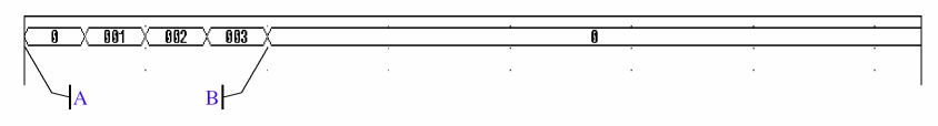
and you want to create a stimulus that consists of three consecutive occurrences of the sequence that starts at A and ends at B:

You can do this by using a standard text editor to edit a stimulus library file. Within this file is a sequence of transitions that produces the original waveform. With a text editor you can modify the stimulus definition so it repeats itself.
To add a loop
- In the Stimulus Editor, save and close the stimulus file.
- In a standard text editor (such as Notepad), open the stimulus file.
- Find the set of consecutive lines comprising the sequence that you want to repeat.
Each relevant line begins with the time of the transition and ends with a value or change in value.
To find out more about the syntax of the stimulus commands used in the stimulus file, refer to the PSpice A/D Reference Guide. - Before these lines, insert a line that uses this syntax:
+ Repeat for n_times
where n_times is one of the following:- A positive integer representing the number of repetitions.
- The keyword FOREVER, which means repeat this sequence for an unlimited number of times (like a clock signal).
- Below these lines, insert a line that uses this syntax:
+ Endrepeat
- From the File menu, choose Save.
Given the example shown on page 3, if you wanted to repeat the sequence shown from point A to point B three times, then you would modify the stimulus file as shown here (added lines are in bold):
+ Repeat for 3
+ +0s 000000000
+ 250us INCR BY 000000001
+ 500us 000000010
+ 750us INCR BY 000000001
+ 1ms 000000000
+ Endrepeat
Using the DIGCLOCK part
The DIGCLOCK part allows you to define a clock signal by using the part’s properties.
For information on how to define a clock signal using the Stimulus Editor with the DIGSTIMn part, see Defining signal transitions.
To define a clock signal using DIGCLOCK
- From Capture’s Place menu, choose Part.
- Place and connect a DIGCLOCK part.
- Double-click the part instance.
- Define the properties as described below.
Table 14-3
For this property... Specify this... DELAY
Time before the first transition of the clock
ONTIME
Time in high state for each period
OFFTIME
Time in low state for each period
STARTVAL
Low state of clock (default:0)
OPPVAL
High state of clock (default: 1)
Using STIM1, STIM4, STIM8 and STIM 16 parts
The STIMn partshave a single pin for connection. STIM1 is used for driving a single net. STIM4, STIM8 and STIM 16 drive buses that are 4, 8 and 16 bits wide, respectively. The properties for all of these parts are the same as those shown in Table 14-4 below.
| Property | Description |
|---|---|
|
WIDTH |
Number of output signals (nodes). |
|
FORMAT |
Sequence of digits defining the number of signals corresponding to a digit in any <value> term appearing in a COMMANDn property definition. Each digit must be either 1, 3, or 4 (binary, octal, hexadecimal, respectively); the sum of all digits in FORMAT must equal WIDTH. |
|
IO_MODEL |
I/O model describing the stimulus’ driving characteristics. |
|
IO_LEVEL |
Interface subcircuit selection from one of the four analog/ digital subcircuits provided with the part’s I/O model. |
|
DIG_PWR |
Digital power pin used by the interface subcircuit. |
|
DIG_GND |
Digital ground pin used by the interface subcircuit. |
|
TIMESTEP |
Number of seconds per clock cycle or step. |
|
COMMAND1- |
Stimulus transition specification statements including time/ value pairs, labels, and conditional constructs. |
When placed, you must connect each part to the wire or bus of the corresponding radix. Generally, you only need to modify the FORMAT, TIMESTEP, and COMMANDn properties.
Typically, each COMMANDn property contains only one command line. It is possible to enter more than one command line per property by placing \n+ between command lines in a given definition. (The n must be lower case and no spaces between characters; spaces may precede or follow the entire key sequence.) Refer to the PSpice A/D Reference Guide for information about command line syntax.
Using the FILESTIMn parts
The FILESTIMn parts have a single pin for connection to the rest of the circuit. FILESTIM1 is used for driving a single net. FILESTIM2, FILESTIM4, FILESTIM8, FILESTIM16 and FILESTIM32 drive buses that are 2, 4, 8, 16 and 32 bits wide, respectively. You must define the digital stimulus specification in an external file. Using this technique, stimulus definitions can be created from scratch or extracted with little modification from another simulation’s output file. Refer to the PSpice A/D Reference Guide for more information about creating digital stimulus specifications and files.
Table 14-5 lists the properties of the FILESTIMn parts. The IO_MODEL, IO_LEVEL, and PSPICEDEFAULTNET properties describing this part’s I/O characteristics are provided with default values that rarely need modification. However, you must define the FILENAME property with the name of the external file containing the digital stimulus specification.
The SIGNAME property specifies the name of the signal inside the stimulus file which becomes the output from the FILESTIMn part. If left undefined, the name of the connected net (generally a labeled wire) determines which signal is used.
| Property | Description |
|---|---|
|
FILENAME |
Name of file containing the stimulus specification. If you do not specify the path to the stimulus file, you must place the file in the folder for the simulation profile for which you are configuring the stimulus.
|
|
SIGNAME |
Name of output signal |
|
IO_MODEL |
I/O model describing the stimulus’ driving characteristics |
|
IO_LEVEL |
Interface subcircuit selection from one of the four AtoD or DtoA subcircuits provided with the part’s I/O model |
|
PSPICEDEFAULTNET |
Hidden digital power and ground pins used by the interface subcircuit. Name of the default net to use. |
For example, a FILESTIMn part can be used to reset a counter, which could appear as shown in Figure 14-1 below.
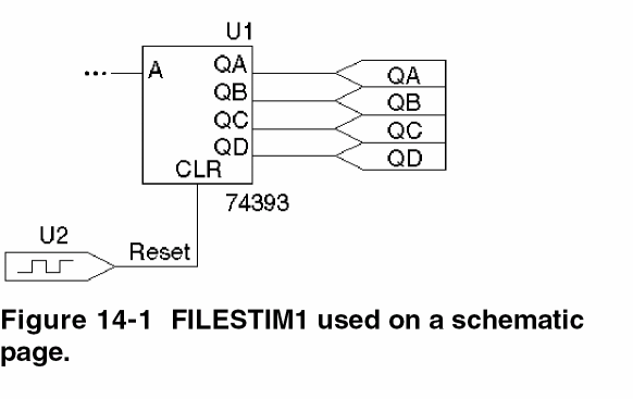
In this case, the FILESTIM1 part instance, U2, generates a reset signal to the CLR pin of the 74393 counter.
To set up the U2 stimulus
The following steps set up the U2 stimulus so that the 74393 counter is cleared after 40 nsec have elapsed in a transient analysis.
- Create a stimulus file named
RESET.STMthat contains the following lines:
Reset
0ns 1
40ns 0
The header line contains the names of all signals described in the file. In this case, there is only one: Reset.
The remaining lines are the state transitions output for the signals named in the header. In this case, the Reset signal remains at state 1 until 40nsec have elapsed, at which time it drops to state 0.
A blank line is required between the signal name list and the first transition. - Place the
RESET.STMfile in the folder for the simulation profile for which you are configuring the stimulus. - Associate this file with the digital stimulus instance, U2, by setting U2’s FILENAME property to
RESET.STM. - Define the signal named Reset in
RESET.STMas the output of U2 by setting U2’s SIGNAME property to Reset. Since the labeled wire connecting U2 with the 74393 counter is also named Reset, it is also acceptable to leave SIGNAME undefined.
Defining simulation time
To set up the transient analysis
- From Capture’s PSpice menu, choose New Simulation Profile.
- Enter a name for the new simulation profile.
- Click OK.
- In the Analysis Type list box on the Analysis tab, select Time Domain (Transient).
- In the Run to Time text box, type the duration of the transient analysis.
- Click OK.
Adjusting simulation parameters
Use the Options tab of the Simulation Settings dialog box to adjust the simulation behavior of your circuit’s digital devices.
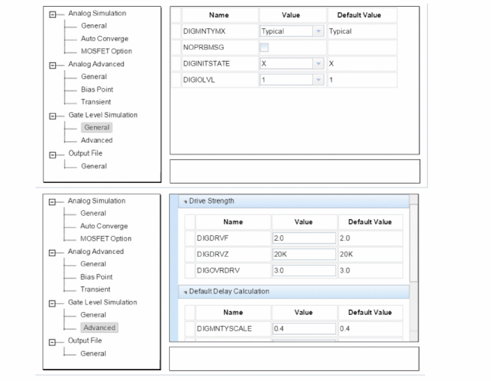
To access the digital settings in the Options tab
- From Capture’s PSpice menu, choose Edit Simulation Profile.
- Click the Options tab.
- In the tree structure, select Gate-level simulation.
Each of the dialog box settings is described in the following sections. For additional options, see Output control options.
Selecting propagation delays
All digital devices—including primitives and library models—perform simulations using either minimum, typical, maximum or worst-case (min/max) timing characteristics. You can set the delay circuit-wide or on individual device instances.
Circuit-wide propagation delays
You can set these to minimum, typical, maximum or variable within the min/max range for digital worst-case timing simulation on the Options tab of the Simulation Settings dialog box.
To specify the delay level circuit-wide
- From Capture’s PSpice menu, choose Edit Simulation Profile.
- Click the Options tab.
- In the Category list box, select Gate-level simulation.
Part instance propagation delays
You can set the propagation delay mode on an individual device, thereby overriding the circuit-wide delay mode.
To override the circuit-wide default on an individual part
- Set the part’s MNTYMXDLY property from 1 to 4 where
1
=
minimum
2
=
typical
3
=
maximum
4
=
worst-case (min/max)
By default, MNTYMXDLY is set to 0, which tells PSpice A/D to use the circuit-wide value defined in the Options tab.
Initializing flip-flops
To initialize all flip-flops and latches
Select one of the three Flip-flop Initialization choices on the Options tab:
-
- If set to X, all flip-flops and latches produce an X (unknown state) until explicitly set or cleared, or until a known state is clocked in.
The X initialization is the safest setting, since many devices do not power up to a known state. However, the 0 and 1 settings are useful in situations where the initial state of the flip-flop is unimportant to the function of the circuit, such as a toggle flip-flop in a frequency divider. - If set to 0, all such devices are cleared.
- If set to 1, all such devices are preset.
- If set to X, all flip-flops and latches produce an X (unknown state) until explicitly set or cleared, or until a known state is clocked in.
Refer to the PSpice A/D Reference Guide for more information about flip-flops and latches.
Starting the simulation
To start the simulation
From the PSpice menu, choose Run.
After PSpice A/D completes the simulation, the graphical waveform analyzer starts automatically.
Analyzing results
PSpice A/D includes a graphical waveform analyzer for simulation results. In effect, the waveform viewer in PSpice A/D is a software oscilloscope. Running PSpice A/D corresponds to building or changing a breadboard, and the waveform viewer corresponds to looking at the breadboard with an oscilloscope. You can observe and interactively manipulate the waveform data produced by circuit simulation.
For mixed analog/digital simulations, the waveform analyzer can display analog and digital waveforms simultaneously with a common time base.
PSpice A/D generates two forms of output: the simulation output file and the waveform data file. The calculations and results reported in the simulation output file are like an audit trail of the simulation. However, the graphical analysis of information stored in the data file is a more informative and flexible method for evaluating simulation results.
To display waveforms
- From the Trace menu, choose Add Trace.
- Select traces for display:
- In the Simulation Output Variables list, click any waveforms you want to display. Each appears in the Trace Expressions box at the bottom.
- Construct expressions by selecting operators, functions and/or macros from the Functions or Macros list, and output variables in the Simulation Output Variables list.
- You can also type trace expressions directly into the Trace Expression text box. A typical set of entries might be:
IN1 IN2 Q1 Q2
Use spaces or commas to separate the output variables you place in the Trace Expressions list.
- Click OK.
Waveforms for the selected output variables appear.
Adding digital signals to a plot
When defining digital trace expressions, you can include any combination of digital signals, buses, signal constants, bus constants, digital operators, macros and the Time sweep variable.
The following rules apply:
- An arithmetic or logical operation between two bus operands results in a bus value that is wide enough to contain the result.
- An arithmetic or logical operation between a bus operand and a signal operand results in a bus value.
The syntax for expressing a digital output variable or expression is:
digital_output_variable[;display_name]
or
digital_expression[;display_name]
| This placeholder... | Means this... |
|---|---|
|
digital_output_ |
output variable from the Simulation Output Variable list (Digital check box selected) |
|
digital_expression |
expression using digital output variables and operators |
|
display_name |
text string (name) to label the signal on the plot, instead of using the default output variable notation |
To add a digital trace expression
- In the Add Traces dialog box, make sure you select the Digital check box.
- Do one of the following:
- In the Simulation Output Variables list, click the signal you want to display.
- In the Trace Expression text box, create a digital expression by either typing the expression, or by selecting digital output variables from the Simulation Output Variables list and digital operators from the Digital Operators and Functions list.
- If you want to label a signal with a name that is different from the output variable:
- Click in the Trace Expression text box after the last character in the signal name.
- Type ;display_name where display_name is the name of the label.
Example:U2:Y;OUT1where U2:Y is the output variable. On the plot, the signal is labeled OUT1.
Adding buses to a waveform plot
You can evaluate and display a set of up to 32 signals as a bus even if the selected signals were not originally a bus. This is done by following the same procedure already given for adding digital signals to the plot. However, when adding a bus, be sure to enclose the list of signals in braces: { }.
{ Q3 Q2 Q1 Q2 }The complete syntax is as follows:
{signal_list}[;[display_name][;radix]]or
{bus_prefix[msb:lsb]}[;[display_name][;radix]]| This placeholder... | Means this... |
|---|---|
|
signal_list |
comma- or space-separated list of up to 32 digital node names, in sequence from high order to low order |
|
bus_prefix[msb:lsb] |
alternate way to express up to 32 signals in the bus |
|
display_name (optional) |
text string (name) to label the bus on the plot, instead of using the default output variable notation To change the radix without changing the display name, be sure to include two consecutive semicolons. Example:
{A3,A2,A1,A0};;radix |
|
radix |
numbering system in which to display bus values |
Valid entries for radix are shown in the following table.
| For this numbering system... | Use this notation... |
|---|---|
|
Binary (base 2) |
B |
|
Decimal (base 10) |
D |
|
Hexadecimal (base 16) |
H or X |
|
Octal (base 8) |
O (the letter) |
To add a bus expression
- In the Add Traces dialog box, in the Functions and Macros list, choose Digital Operators and Constants.
- Click the
{ }entry. - In the Simulation Output Variables list, select the signals in high-order to low-order sequence.
- If you want to label the bus with a name that is different from the default:
- Click in the Trace Expression text box after the last character in the bus name.
- Type ;display_name where display_name is the name of the label.
- If you want to set the radix to something different from the default:
- Click in the Trace Expression text box after the last character in the expression.
- Type one of the following where radix is a value from Table 14-8:
- If you specified a display_name, then type ;radix.
- If you did not specify a display_name, then type ;;radix (two semicolons preceding the radix value).
Examples:
{Q2,Q1,Q0};A;Ospecifies a 3-bit bus whose most significant bit is Q2. PSpice A/D labels the plot A, and values appear in octal notation.{a3,a2,a1,a0};;dspecifies a 4-bit bus. On the plot, values appear in decimal notation. Since no display name is specified, PSpice A/D uses the signal list as a label.{a[3:0]}is equivalent to{a3,a2,a1,a0}
Tracking timing violations and hazards
When there are problems with your design, such as setup/hold violations, pulse-width violations, or worst-case timing hazards, PSpice A/D saves messages to the simulation output file or data file. You can select messages and have the associated waveforms and detailed message text automatically appear.
PSpice A/D can also detect persistent hazards that may have a potential effect on a primary circuit output or on the internal state of the design.
Persistent hazards
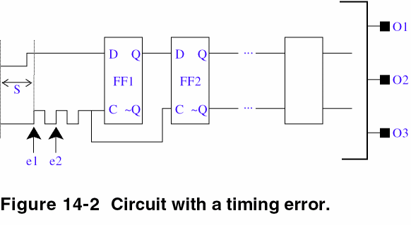
Digital problems are usually either timing violations or timing hazards. Timing violations include SETUP, HOLD and minimum pulse WIDTH violations of component specifications. This type of violation may produce a change in the state behavior of the design, and potentially in the answer. However, the effects of many of these errors are short-lived and do not influence the final circuit results.
For example, consider an asynchronous data change on the input to flip-flop FF1 in Figure 14-2 below. The data change is too close to the clock edge e1, resulting in a SETUP violation. In a hardware implementation, the output of FF1 may or may not change. However, some designs are not sensitive to this individual missed data because the next clock edge (e2 in this example) latches the data. The designer must judge the significance of timing errors, accounting for the overall behavior of the design.
Timing hazards are most easily identified by simulating a design in worst-case timing mode, usually close to its critical timing limits. Under such conditions, PSpice A/D reports conditions such as AMBIGUITY CONVERGENCE hazards. Again, these may or may not pose a problem to the operation of the design.
However, there are identifiable cases that cause major problems. An example of a major problem is shown in Figure 14-3 below. Due to the simultaneous arrival of two timing ambiguities (having unrelated origins, therefore nothing in common) at the inputs to gate G1, PSpice A/D reports the occurrence as an AMBIGUITY CONVERGENCE hazard. This means that the output of G1 may glitch.
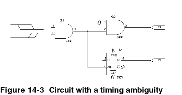
Note that the output fans out to two devices, G2 and L1. The effects of a glitch on G1 in this case do not reach the circuit output P1, because that path is not sensitized (since the other input to G2 is held LO and thus blocks the symptom). However, because G1’s output is also used to clock latch L1, the effects of a glitch could result in visibly incorrect behavior on output P2. This is an example of a persistent hazard.
A persistent hazard is a timing violation or hazard that has a potential effect on a primary (external) circuit output or on the internal state (stored state or memory elements) of the design. For the design to be considered reliable, you must correct such timing hazards.
PSpice A/D fully distinguishes between state uncertainty and time uncertainty. When a hazard occurs, PSpice A/D propagates hazard origin information along with the machine state through all digital devices. When a hazard propagates to a state-storage device primitive (JKFF, DFF, SRFF, DLTCH, RAM), PSpice A/D reports a PERSISTENT HAZARD.
Simulation condition messages
PSpice A/D produces warning messages in various situations, such as those that originate from the digital CONSTRAINT devices monitoring timing relationships of digital nodes. These messages are directed to the simulation output file and/or to the waveform data file. Options are available for controlling where and how many of these messages are generated, as summarized later in this section.
Table 14-9 and 14-10 below summarizes the simulation message types, with a brief description of their meaning. Currently, the messages supported are specific to digital device timing violations and hazards.
| Message type | Severity level | Meaning |
|---|---|---|
|
SETUP |
WARNING |
Minimum time required for a data signal to be stable prior to the assertion of a clock was not met. |
|
HOLD |
WARNING |
Minimum time required for a data signal to be stable after the assertion of a clock was not met. |
|
RELEASE |
WARNING |
Minimum time required for a signal that has gone inactive (usually a control such as CLEAR) to remain inactive before the asserting clock edge was not met. |
|
WIDTH |
WARNING |
Minimum pulse width specification for a signal was not satisfied; that is, a pulse that was too narrow was observed on the node. |
|
FREQUENCY |
WARNING |
Minimum or maximum frequency specification for a signal was not satisfied. Minimum frequency violations indicate that the period of the measured signal is too long, while maximum frequency violations describe signals changing too rapidly. |
|
GENERAL |
INFO |
Boolean expression described within the GENERAL constraint checker was evaluated and produced a true result. |
| Message type | Severity level | Meaning |
|---|---|---|
|
AMBIGUITY |
WARNING |
Convergence of conflicting rising and falling states (timing ambiguities) arrived at the inputs of a primitive and produced a pulse (glitch) on the output. |
|
CUMULATIVE |
WARNING |
Signal ambiguities are additive, increased by propagation through each level of logic in the circuit. The ambiguities associated with both edges of a pulse increased to the point where they overlapped, which PSpice A/D reports as a cumulative ambiguity hazard. |
|
SUPPRESSED GLITCH |
WARNING |
Pulse applied to the input of a primitive that is shorter than the active propagation delay was ignored by PSpice A/D; significance depends on the nature of the circuit. There might be a problem either with the stimulus, or with the path delay configuration of the circuit. |
|
NET-STATE CONFLICT |
WARNING |
Two or more outputs attempted to drive a net to different states, which PSpice A/D reports as an X (unknown) state. This usually results from improper selection of a bus driver’s enable inputs. |
|
ZERO-DELAY- |
FATAL |
Output of a primitive changed more than 50 times within a single digital time step. PSpice A/D aborted the run. |
|
DIGITAL INPUT |
SERIOUS |
Voltage on a digital pin was out of range, which means PSpice A/D used the state with a voltage range closest to the input voltage and continued the simulation. |
|
PERSISTENT HAZARD |
SERIOUS |
Effects of any of the aforementioned logic hazards were able to propagate to either an external port or to any storage device in the circuit. See Persistent hazards for more information. |
Output control options
Four control options are available for managing the generation of simulation condition messages. These are described in Table 14-11.
To access these commands, select the Options tab in the Simulation Settings dialog box. You can set NOOUTMSG and NOPRBMSG by selecting the Output file option. You can set DIGERRDEFAULT and DIGERRLIMIT by selecting the Gate-level simulation tree structure.
| This option... | Means this... |
|---|---|
|
NOOUTMSG |
Suppresses the recording of simulation condition messages in the simulation output file. |
|
NOPRBMSG |
Suppresses the recording of simulation condition messages in the waveform data file. |
|
DIGERRDEFAULT=<n> |
Establishes a default limit, n, to the number of condition messages that may be generated by any digital device that has a constraint checker primitive without a local default. If global or local defaults are unspecified, there is no limit. |
|
DIGERRLIMIT=<n> |
Establishes an upper limit, n, for the total number of condition messages that may be generated by any digital device. If this limit is exceeded, PSpice A/D aborts the run. By default, the total number of messages is 20. |
Severity levels
PSpice assigns one of four severity levels to the messages:
- FATAL
- SERIOUS
- WARNING
- INFO (informational)
FATAL conditions cause PSpice A/D to cancel the simulation. Under all other severity levels, PSpice A/D continues to run. The severity levels are used to filter the classes of messages that are displayed when loading a data file.
View the next document: 15 - Mixed Analog/Digital Simulation
If you have any questions or comments about the OrCAD X platform, click on the link below.
Contact Us