PCB Component Placement Guide with OrCAD X
Key Takeaways
-
The guide features a step-by-step approach, starting with major components and using alignment tools to ensure an organized layout.
-
Adjusting visibility settings in OrCAD X, including layer colors and Quick View, improves workspace clarity for efficient placement.
-
OrCAD X features like cross-probing, series mode, and 3D visualization enhance precision and placement efficiency.
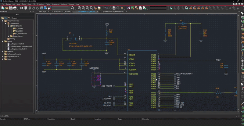
OrCAD X drag and drop component placement from Capture
This PCB component placement guide outlines effective techniques for PCB component placement in OrCAD X, focusing on integrating functional design with manufacturing requirements. We explore practical methods, key design considerations, and how OrCAD X features streamline the PCB layout process.
PCB Component Placement Considerations
Modern PCB design demands precise component placement to meet complex functional and manufacturing requirements. With higher circuit density and reduced board space, designers must carefully balance signal integrity, thermal management, and manufacturability.
Functional PCB Component Placement Considerations
-
Floor Planning: Begin with a clear partitioning of digital, analog, RF, and power sections to isolate noise and maintain signal integrity.
-
Routing Efficiency: Place high-speed components close together to minimize trace length and maintain clear return paths.
-
Thermal Management: Position heat-generating devices (e.g., processors) centrally to ensure even heat dissipation, while allowing room for decoupling capacitors, heat sinks, and proper airflow.
-
Accessibility: Ensure that components remain accessible for testing and future upgrades, avoiding placements that hinder technician rework.
Manufacturing Considerations for PCB Component Placement
-
Assembly Requirements:
-
Wave Soldering: Maintain clearance between SMT parts and thru-hole connectors, and orient pins perpendicular to the solder wave to ensure consistent solder joints.
-
Reflow Soldering: Ensure balanced thermal profiles for multi-pin parts to prevent tombstoning.
Testability: Include appropriately spaced test points for ICT or flying probe testing.
Panelization and Coating: Account for board break-out tabs and conformal coating by ensuring sufficient edge clearance.
Before Placement: Getting Started, Visibility, and Best Practices
Before starting the physical placement, adjust your visibility options to optimize the workspace.
Visibility Pane Adjustments
Use the left-hand visibility pane to toggle the display of layers and objects. Customize the appearance of your layout editor, OrCAD X Presto by:
-
Assigning Colors: Right-click the ‘All’ option and select Rainbow Down to automatically assign distinct colors to all copper layers—ideal for complex, multi-layer designs.
-
Customizing Colors Specific Layers: Solder Mask, Silkscreen, Paste Mask, DRC (Design Rule Checks)
-
Toggle off redundant geometries by right-clicking them.
-
Component-Specific Settings: In the component section, adjust the assembly color (e.g., to light blue) and activate the Quick View option which displays a clear reference designator on each component
-
Manufacturing Options: At the bottom of the visibility pane, enable the view for plated holes, back drill holes, unplated holes, and petal holes.
Best Practices for Component Placement
-
Pre-Layout Verification: Always verify board dimensions, layer stack-up, and keep-out zones before placing components.
-
Standardization: Maintain consistent pin 1 orientation across all components to reduce placement errors.
-
Documentation: Compile documentation packages for manufacturers to minimize bottlenecks in production.
Before moving on to placement, review your design for assembly rules. These rules are critical when specific spacing or proximity restrictions apply between component types.
Step-by-Step PCB Component Placement Guide
|
Step |
Action |
Details |
|
1. Adjust Visibility |
Open the visibility pane; set colors and toggle objects. |
Customize solder mask, silkscreen, paste mask, and set your DRC rules. Enable Quick View to display component reference designators, and toggle off redundant geometries and nets as needed. |
|
2. Initiate Placement |
Right-click on the ‘Move’ command and select Place. |
Access the placement command from the context menu. Use the helper window (toggle with the X key or click the “Place” tab) to access additional placement options. |
|
3. Load Components for Placement |
Use various methods to load components. |
By Reference: Enter a reference (e.g., C32) in the text field so the component hovers under your cursor. From List: Highlight unplaced components (using Ctrl+A or Shift-click) in the search window. Series Mode: Type a range or a comma-separated list to load components in reference order. Cross-Probing: Select parts in the schematic (using parts filter and box-select) to have them highlighted in OrCAD X. |
|
4. Place Major Components First |
Place large components to establish design anchors. |
Start with major components (such as connectors and the main IC) to establish anchor points. Then, use schematic references to group and sequentially place smaller parts. |
|
5. Manipulate Components |
Move, rotate, mirror, align components as needed. |
Move: Place components within the board outline using the move command. Rotate: Press the R key or adjust rotation via the properties dropdown. Mirror: Press the M key or select the mirror option in the properties window to flip components between top and bottom layers. Align: Use object snapping or alignment guides to ensure precise placement. |
|
6. Manage Workspace Clutter |
Hide net connections (ratsnests) to reduce visual clutter. |
Toggle off net visibility through the Nets section in the visibility pane or by right-clicking on specific nets (e.g., power nets). Re-enable these later during the routing review for checking interconnections. |
|
7. Switch Between 2D and 3D Views |
Activate 3D view from the Display section. |
Switch to 3D view to verify component placement. Choose between viewing components via bound extrusion or STEP model representations for a realistic physical check. |
|
8. Final Verification |
Review the layout for placement accuracy and prepare for routing. |
Ensure all components are within the board outline (status should show “0 unplaced”). Examine the layout in both 2D and 3D views to identify overlaps or spacing issues (e.g., “bow tie” formations) and adjust misalignments before proceeding to routing and constraint setup. |
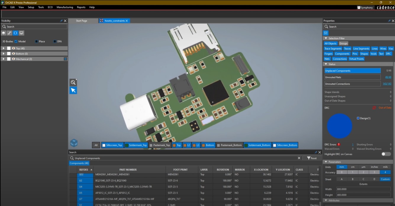
OrCAD X 3D Visualization to Verify Component Placement
PCB Component Placement Verification in OrCAD X
OrCAD X features can help you place your component easily, utilizing advanced alignment tools, cross-probing between schematic and layout, and real-time 3D visualization to streamline your PCB design process.
OrCAD X Features to Guide Component Placement
|
Feature |
Description |
|
Verifies schematic completeness and layout correctness before starting placement. |
|
|
Sets up board layer stack-up and verifies all layer details. |
|
|
Helps define physical spacing and component placement rules to ensure design integrity. |
|
|
Constraint-Driven Placement |
Enables rule-based grouping of components according to functional blocks. |
|
Provides 3D visualization for spatial awareness of component interaction and layout refinement. |
This PCB component placement guide should help you optimize your design in OrCAD X to ensure every design detail meets your performance and manufacturability goals. With OrCAD X, you can precisely position components and fine-tune your layout with ease. Discover how Cadence’s PCB Design and Analysis Software tools can transform your design process—learn more today.
Leading electronics providers rely on Cadence products to optimize power, space, and energy needs for a wide variety of market applications. To learn more about our innovative solutions, subscribe to our newsletter or subscribe to our YouTube channel.