How to Set Up Design Constraints
Key Takeaways
-
OrCAD X Constraint Manager enables a rules-driven PCB design process by enforcing standardized constraints.
-
Using Constraint Sets (CSETS) allows designers to efficiently apply predefined rules to multiple nets, streamlining the PCB layout process and maintaining consistency.
-
Enabling design rule checks ensures that constraints, such as differential pair rules, are consistently enforced during PCB layout.
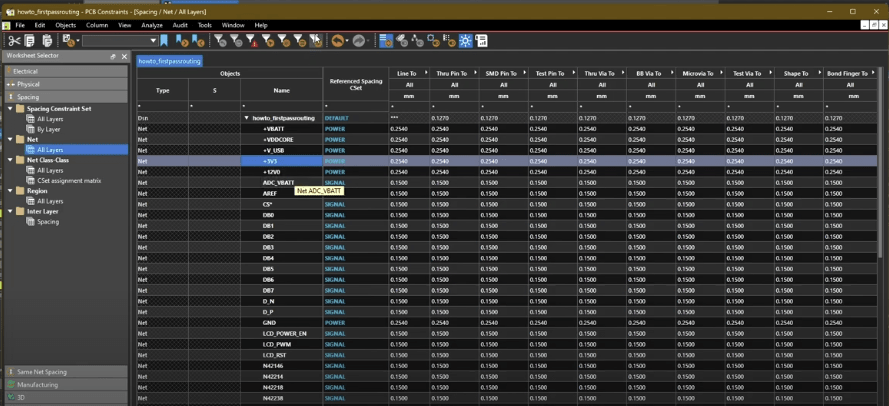
Spacing Constraints in OrCAD X.
Design constraints define the electrical, physical, and manufacturing rules that guide the development of a printed circuit board (PCB), ensuring that your design meets functional, reliability, and manufacturability requirements. Without well-defined constraints, PCBs may suffer from electrical integrity issues, mechanical failures, or production inefficiencies, leading to costly redesigns and delays–hence why it is important to know how to set up design constraints.
Categories of Design Constraints
|
Constraint Type |
Description |
|
Electrical |
Define signal integrity parameters such as impedance control, propagation delays, differential pair rules, and matched-length routing. These constraints help ensure proper signal transmission and reduce noise or cross-talk in high-speed designs. |
|
Physical |
Govern the geometrical aspects of the PCB, such as trace widths, via sizes, and layer stack-ups. Proper physical constraints are critical for ensuring current capacity, thermal performance, and mechanical durability. |
|
Spacing |
Specify minimum clearances between different objects (traces, vias, pads) to avoid short circuits and ensure compliance with manufacturing capabilities. |
|
Manufacturing |
Enforce design rules that align with fabrication and assembly processes, ensuring that the PCB can be reliably produced without yield losses. |
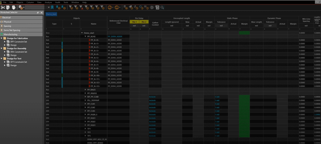
How to Set Up Design Constraints in OrCAD X Constraint Manager
OrCAD X provides a dedicated Constraint Manager, which serves as a central hub for defining and managing all design constraints. It allows designers to establish and apply rules efficiently across the PCB layout, ensuring a rules-driven design approach. Accessing the Constraint Manager in OrCAD X is straightforward:
-
Navigate to Tools > Constraint Manager from the main menu.
-
The Constraint Manager interface is divided into multiple sections based on different constraint types.
OrCAD X Constraint Management Tool
Key Features of the Constraint Manager:
-
Electrical Constraints: Includes high-speed design parameters like target impedance, propagation delays, differential pair settings, and matched length constraints.
-
Physical Constraints: Controls aspects such as trace width, via sizes, and neck-down constraints for routing optimization.
-
Spacing and Same Net Spacing: Defines clearance rules between different design objects to ensure proper signal isolation and manufacturability.
-
Constraint Sets (CSETS): Instead of manually configuring constraints for each net, designers can define reusable Constraint Sets (CSETS) and apply them across multiple nets or regions. This significantly improves design efficiency and consistency.
-
Technology Files (*.tcfx): OrCAD X allows users to create and save technology files that store predefined constraint settings, enabling standardization across multiple projects.
Setting Up Electrical Constraints and Physical Constraints
As mentioned, OrCAD X allows you to define various design constraints to ensure your PCB meets electrical and manufacturing requirements. For this article, we'll walk through an example of how to set up design constraints to implement a differential pair in your design.
Configuring Electrical Constraints
Electrical constraints must be defined for differential pairs to ensure proper signal integrity and performance in high-speed designs.
-
Creating an Electrical Constraint Set
-
In the Worksheet Selector, choose the Electrical Domain.
-
Expand the Electrical Constraint Set > Routing > Differential Pair worksheet.
-
Right-click in the table and select Create Electrical CSET.
-
Name the constraint set DP and click OK.
Defining Electrical Parameters
-
Set Gather Control to Ignore to exclude the etch length from pin to gather point when calculating Max uncoupled length.
-
Set Maximum Uncoupled Length to 5.08 mm.
-
Set Static Phase Tolerance to 0.508 mm.
-
Press Enter or Tab to move to the next cell and save the changes.
Assigning Electrical Constraints to Differential Pair Nets
-
Expand the Net > Routing > Differential Pair worksheet.
-
In the Reference Electrical CSET column for your differential pair object, select the DP constraint set.
-
Assigning this constraint set at the top level applies the associated rules to each net in the differential pair.
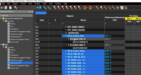
Assigning your Electrical Constraints to Differential Pair Nets in OrCAD X
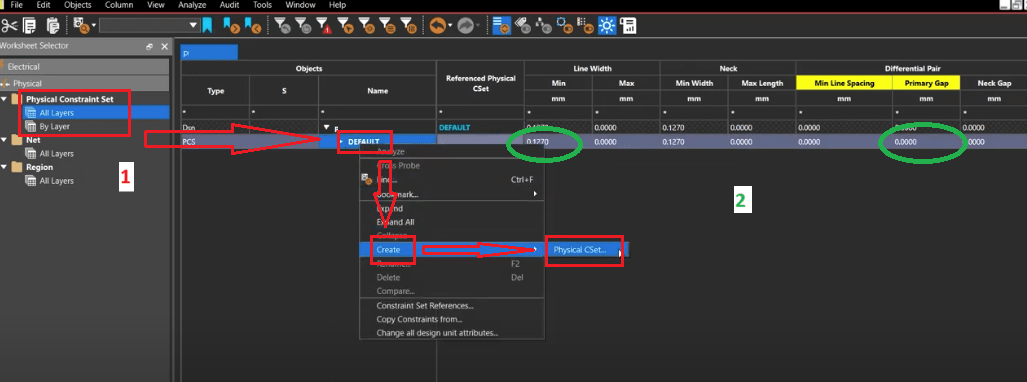
Configuring Physical Constraints
Defining physical constraints ensures that the differential pair follows the necessary width and spacing rules during PCB layout.
-
Creating a Physical Constraint Set
-
In the Worksheet Selector, choose the Physical Domain.
-
Expand the Physical Constraint Set > All Layers worksheet.
-
Right-click the Default Constraint Set and select Create Physical CSet.
-
Name the constraint set DP and click OK.
Defining Physical Parameters
-
Set Minimum Line Width to 0.127 mm.
-
Set Primary Gap to 0.127 mm.
Assigning Physical Constraints to Differential Pair Nets
-
Select the Net > All Layer worksheet in the Physical Domain.
-
In the Reference Physical CSet column for your differential pair object, select the DP constraint set.
Setting Electrical Constraints in OrCAD X
Enabling Design Rule Checks for Differential Pairs
To automatically validate differential pair constraints during PCB layout:
-
Select Analyze > Analysis Modes from the Constraint Manager menu.
-
From the Analysis Modes list, choose Electrical.
-
Check the box for All Differential Pair Checks to activate constraint verification.
-
Click Apply, then OK, and close the Constraint Manager.
Reviewing Constraints in the OrCAD X Presto Canvas
-
Open the Properties Panel in the OrCAD X Presto canvas.
-
Under Selection Filter, select All Objects to turn everything off.
-
Select Nets to filter only net objects.
-
Select Net D- from X1.
-
In the Properties Panel, switch to Constraints Mode to view assigned electrical and physical constraints.
-
To restore visibility, select All Objects under the Selection Filter.
By following these steps, you can ensure your differential pairs meet design requirements and maintain signal integrity throughout the PCB layout process in OrCAD X.
With that, you should have a place to get started with how to set up design constraints in OrCAD X, a crucial step in ensuring a successful PCB layout. With powerful constraint management tools, designers can define electrical, physical, spacing, and manufacturing rules to optimize signal integrity, manufacturability, and overall performance. Whether you're working with high-speed signals or complex board geometries, OrCAD X provides the flexibility needed to enforce critical design rules. To learn more about how to set up design constraints and explore Cadence’s full suite of PCB Design and Analysis tools, visit the OrCAD X platform and take advantage of industry-leading solutions for your next project.
Leading electronics providers rely on Cadence products to optimize power, space, and energy needs for a wide variety of market applications. To learn more about our innovative solutions, subscribe to our newsletter or our YouTube channel.