PCB Design Specifications for Beginner Engineers
Key Takeaways
-
Essential PCB design specifications include controlling current capacity and impedance; which is key in preventing electrical arcing and crosstalk.
-
Choose the appropriate via type, accounting for aspect ratios, tenting, and plugging for reliability.
-
Select materials and layer arrangements to optimize signal integrity, thermal performance, and manufacturability.
Line spacing and line width are important PCB design specifications for efficient manufacturing and effective performance.
Understanding PCB design specifications is important for beginner engineers and those entering their circuit board design journey. This guide delves into common PCB design specifications, discussing common manufacturer requirements, and an overview of the need-to-know basics of PCB design specifications.
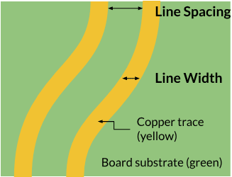
Line Width and Spacing
Line width and spacing influence current-carrying capacity, impedance, and overall board density.
-
Line Width: Determines the amount of current a trace can safely carry without excessive heating. Wider traces are used for power and ground paths, while signal traces can be narrower.
-
Line Spacing: The distance between adjacent traces must prevent electrical arcing and crosstalk, especially in high-frequency designs.
Key considerations:
-
Current Requirements: Use IPC-2152 guidelines to calculate appropriate line widths for the expected current.
-
Impedance Control: For high-speed signals, precise line widths are necessary to maintain characteristic impedance.
-
Manufacturing Limitations: Fabricators have minimum trace width and spacing capabilities, often around 0.075 mm (3 mils) for standard processes.
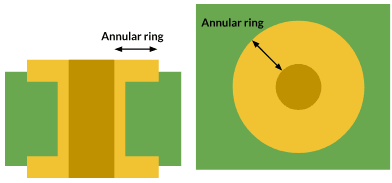
Annular ring summary diagram
Annular Ring
An annular ringis the ring of copper around a plated through-hole (via) on a PCB. It is critical for ensuring reliable electrical connections between layers.
-
Minimum Annular Ring: The smallest allowable width of the ring to ensure structural integrity and electrical reliability.
-
Design for Manufacturing: Account for drill wander and registration tolerances to prevent breakout, where the hole encroaches on the pad edge.
Standard specifications recommend a minimum annular ring width of 0.05 mm to 0.1 mm, but this may vary based on fabrication capabilities and board requirements.
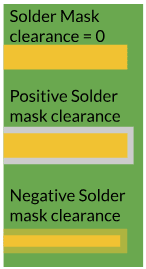
Solder mask clearance summary diagram
Solder Mask Clearance
The solder mask is a protective layer that prevents solder bridging and protects copper traces from environmental damage.
-
Solder Mask Clearance is the intentional gap between the solder mask and the pads or traces it surrounds.
-
Positive Clearance: Exposes more pad area, which is useful for hand soldering.
-
Negative Clearance: Covers more of the pad, which is helpful in preventing solder wicking.
-
Solder Mask Dam: The narrow strip of solder mask between closely spaced pads, crucial in preventing shorts between pins of fine-pitch components.
Key design points include:
-
Common manufacturing tolerances allow for a typical solder mask expansion of 0.05 mm to 0.075 mm beyond the copper feature.
- Choose solder mask openings based on component footprints, component type, and assembly methods.
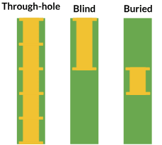
Different via types summary diagram
Via Design and Placement
Vias are used to create electrical connections between different layers of a PCB. Via Types include:
-
Through-Hole Vias: Extend from the top to the bottom layer.
-
Blind Vias: Connect outer layers to one or more inner layers.
-
Buried Vias: Connect inner layers without reaching the outer surfaces.
When choosing an appropriate via, consider:
-
Aspect ratio, which is the ratio of the PCB thickness to the diameter of the via. This affects manufacturability and lower aspect ratios (<10:1) are preferred.
-
Via tenting and plugging are additional features that determine via function:
-
Tenting: Covering vias with soldermask to prevent contamination.
-
Plugging: Filling vias with resin or conductive material for reliability in high-density designs.
Designers should specify via sizes and types that align with both electrical requirements and manufacturing capabilities.
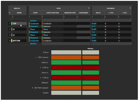
Cross-section editor and associated stackup of a 4 layer board in OrCAD X
Material and Layer Stack-Up
Selecting appropriate materials and defining the layer stack-up are important for overall board function and reliability.
-
Substrate Material: FR-4 is standard, but alternatives like Rogers materials are used for high-frequency applications.
-
Dielectric Constants: Affects signal speed and impedance calculations.
-
Layer Count: Determined by circuit complexity and routing density.
Specifications should detail:
-
Material Types: Including flame retardancy ratings and thermal properties if needed.
-
Thicknesses: Of both dielectric layers and copper foil.
-
Order of Layers: Arrangement of signal, power, and ground layers to optimize performance.
Surface Finishes
The choice of surface finish impacts solderability, shelf life, and cost.
-
HASL (Hot Air Solder Leveling): Economical but uneven surface, not ideal for fine-pitch components.
-
ENIG (Electroless Nickel Immersion Gold): Provides a flat surface and good solderability but is more expensive.
-
OSP (Organic Solderability Preservative): Cost-effective with a limited shelf life.
Designers should specify a surface finish that aligns with assembly requirements and budget considerations.
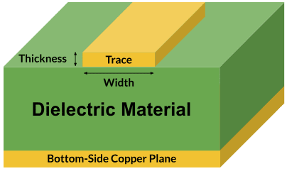
Diagram illustrating trace thickness and width
Copper Thickness
Copper thickness refers to the thickness of the copper layer on a PCB and is typically measured in ounces per square foot (oz/ft²). The standard thicknesses range from 1 oz/ft² (35 µm) to 2 oz/ft² (70 µm), but other values can be specified based on the application's current-carrying requirements.
-
Current Capacity: Thicker copper allows for higher current to flow through the traces without excessive heat buildup.
-
Thermal Management: Increased copper thickness also improves the board's ability to dissipate heat, helping with thermal management.
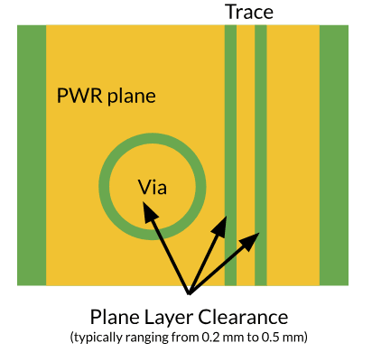
Plane layer clearance summary diagram.
Power and Ground Plane Layer Clearance
Plane layers, typically used for power and ground connections, are areas of copper that provide low-resistance paths and also help in heat dissipation. Plane layer clearance refers to the gap between the plane and other conductive elements not electrically connected to it, such as a via that goes through a plane.
-
Electrical Isolation: Adequate clearance prevents short circuits and electrical interference between different nets.
-
Manufacturing Tolerances: Clearances must account for etching tolerances during PCB fabrication to avoid unintended connections.
-
Regulatory Compliance: Safety standards may dictate minimum clearances, especially in high-voltage applications.
Designers should specify clearances that meet both electrical requirements and manufacturing capabilities, typically ranging from 0.2 mm to 0.5 mm, but adjusted as needed based on specific constraints.
Advanced PCB Design Specifications
If your board requires high-speed or high-power components, further design specifications should be accounted for.
Controlled Impedance and Signal Integrity
For high-speed and high-frequency circuits, maintaining signal integrity through controlled impedance is crucial. See our controlled impedance design guide for more detailed information.
-
Trace Geometry: Line width, thickness, and spacing relative to reference planes determine impedance.
-
Dielectric Material Stack-Up Configuration: The properties of the PCB substrate affect signal propagation in addition to the layer arrangement.
Specifications should include:
-
Impedance Tolerance: Typically ±10%, but tighter tolerances may be required for critical applications.
-
Test Coupons: Included in the design for impedance validation during manufacturing.
Thermal Management and Relief Pads
Effective thermal management ensures the longevity and reliability of electronic components.
-
Use dedicated layers or areas to dissipate heat from high-power components.
-
Implement arrays of thermal vias to conduct heat to internal planes or the opposite side of the PCB.
-
High thermal conductivity substrates like metal-core PCBs can be specified for enhanced heat dissipation.
Design specifications should address thermal requirements, including maximum operating temperatures and cooling methods. Thermal relief pads help solder large components or pins that are connected to large copper areas like ground or power planes. Without thermal relief, the large copper planes can act as heat sinks, drawing away heat and making it difficult to form proper solder joints during assembly.
-
Thermal relief pads consist of thin traces (spokes) that connect the pad to the plane, reducing the heat dissipation into the copper plane and allowing the pad to heat up more evenly during soldering.
-
Controlling the thermal flow, these pads help ensure proper soldering of components, preventing cold joints that can affect the reliability of the connection.
-
Designers can adjust the number and width of the thermal relief spokes to suit the specific thermal characteristics of the board and components.
Using thermal relief pads ensures better soldering results and enhances the overall reliability of the PCB, especially in designs with large copper planes.
Working with OrCAD X For PCB Design Specifications
Clear communication of these specifications to fabrication and assembly partners is essential for the successful realization of electronic products. Below we’ve summarized how OrCAD X can help:
|
PCB Design Specification |
OrCAD X Support |
|---|---|
|
Controlled Impedance and Signal Integrity |
- Constraint Manager: OrCAD X allows setting up impedance constraints easily through the constraint manager. It helps in maintaining controlled impedance by providing real-time constraint-driven feedback during routing. |
|
Thermal Management and Relief Pads |
- Via Arrays: Designers can create via arrays tailored for thermal management using OrCAD X tools, ensuring ideal heat dissipation. |
|
Stack-Up Configuration |
- Cross-Section Editor: OrCAD X provides a powerful cross-section editor for defining the stack-up of a PCB with precise control over layer materials, thicknesses, and other critical properties. |
By thoroughly understanding these PCB design specifications, engineers can ensure that their designs meet performance goals and manufacturing constraints. From detailed stack-up configurations to real-time design rule checks, OrCAD X helps engineers create high-quality PCBs that meet both electrical and manufacturing requirements. Explore our full range of PCB Design and Analysis Software and see how OrCAD X can enhance your next design.
Leading electronics providers rely on Cadence products to optimize power, space, and energy needs for a wide variety of market applications. To learn more about our innovative solutions, subscribe to our newsletter or subscribe to our YouTube channel.