PCB Design Testability: A Practical Guide for Beginners
When you're designing your first printed circuit board (PCB), it's easy to become consumed by functionality, layout, and part selection. However, one crucial aspect that often slips through the cracks is testability. Without proper planning for how your board will be verified and validated, even the most elegantly routed design can become a nightmare to debug, inspect, and scale to production.
Testability affects everything from yield and reliability to production cost. In fact, testing can account for up to 30 percent of a PCB's total production expense. By applying Design for Testability (DFT) principles early in your design cycle, you can minimize defects, streamline manufacturing, and create a board that is far easier to evaluate throughout its life cycle. DFT is not a separate task that happens after layout; it is a design philosophy that enables your boards to be inspected, measured, and verified every step of the way.
What Does It Mean to Design for Testability (DFT)?
Design for Testability refers to a set of techniques and layout decisions that ensure key circuits can be accessed, measured, and evaluated during different phases of manufacturing and usage. This includes everything from electrical test points and component placement to design partitioning and support for automated testing methods.
A board that is easy to test tends to be easier to debug, validate, and eventually scale into volume production. It allows technicians to detect shorts, opens, and component failures early. It also gives engineers visibility into how the circuit is performing under real-world conditions.
There are several types of testing used in PCB manufacturing and validation. Each serves a specific purpose, and understanding how your board will be tested is essential when deciding how to lay it out.
Common PCB Testing Methods
|
Testing Method |
Purpose |
Key Details |
|
Bare Board Testing |
Verifies copper connectivity and isolation before assembly |
Includes continuity tests for net connections and hi-pot tests for insulation resistance. Can be performed using flying probe (flexible but slower) or fixture-based systems (faster but more costly). |
|
In Circuit Testing (ICT) |
Detects shorts, opens, and incorrect component values post-assembly |
Uses a bed-of-nails fixture. Best for high-volume production. Requires consistent test pad size, spacing, and fiducials for alignment. |
|
Flying Probe Testing |
Electrically tests assembled boards without a fixture |
Ideal for prototypes and low-to-medium volume. Requires open access to test points and appropriate spacing. Can probe both top and bottom layers. |
|
Functional Testing |
Evaluates the board under real-world operating conditions |
Checks system behavior while powered. Needs firmware access, I/O ports, and interfaces for stimulation and observation. |
|
Boundary Scan (JTAG) |
Tests internal digital connections through scan chains |
Useful for dense digital systems. Requires support for IEEE 1149.1 standard and accessible JTAG headers. |
|
Visual / AOI / Xray Inspection |
Identifies assembly defects such as misalignment or poor solder joints |
Manual inspection is prone to error. Automated Optical Inspection (AOI) and X-ray improve detection accuracy, especially for hidden joints or dense boards. |
Bare board testing is usually the first step, performed before components are assembled. This checks for continuity and isolation on copper layers, ensuring that no opens or shorts are present. These tests are typically performed using flying probe testers or fixture-based systems, depending on the production volume.
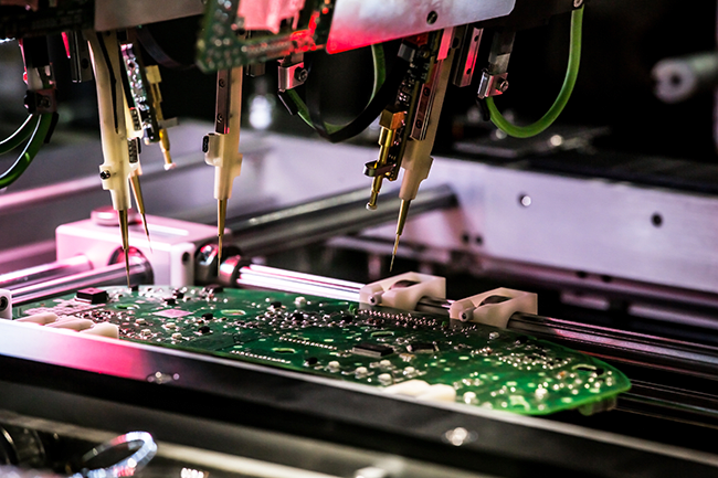
In-circuit testing, or ICT, comes into play after assembly. It uses a fixture known as a bed-of-nails to apply probes to specific points on the board. ICT is very effective at catching component faults, incorrect values, or soldering issues. However, it requires test access to be pre-planned and designed into the board, with enough clearance and consistent pad sizing to support the fixture.
Flying probe testing is a flexible alternative that does not require a fixture. Instead, robotic probes move from point to point, testing the board dynamically. This method is slower but far more economical for prototypes and low-volume runs. It still requires that test points be reachable and well spaced.
Functional testing evaluates the board in an active state. Power is applied, and signals are monitored or stimulated to confirm that the system behaves as expected. This may involve custom firmware, test jigs, or the use of debug interfaces such as UART, I2C, or SPI headers. It provides the most realistic validation, especially for embedded systems.
For digital designs with complex signal paths, boundary scan testing using JTAG is a powerful option. This method allows test signals to be passed internally through a scan chain of devices, giving deep insight without relying on external probes. It requires support for the IEEE 1149.1 standard and the inclusion of accessible JTAG headers on the board.
In addition to electrical tests, many production workflows include visual inspection. This may be performed manually or with automated optical inspection (AOI) systems. AOI uses cameras to detect missing, misaligned, or poorly soldered components. For boards with dense features or hidden joints, X-ray inspection is often used to evaluate solder connections under BGAs or through vias.
Environmental and Stress Testing for Long-Term Reliability

In addition to verifying electrical connectivity and function, it's important to evaluate how a PCB performs under real-world environmental and mechanical stress. These stress tests help uncover latent defects that may not appear during standard in-circuit or functional testing. While not always performed during prototype validation, they are essential for production-grade designs that must withstand temperature variation, vibration, moisture, or mechanical strain.
One of the most common stress tests is thermal cycling, which repeatedly exposes the board to extreme hot and cold conditions. This simulates real-world temperature swings and helps reveal solder fatigue, microcracks, or material delamination that may occur over time. Vibration testing is also critical, especially for automotive, aerospace, or industrial electronics, where sustained motion can weaken joints and connectors.
Boards may also be subjected to humidity and corrosion tests, which simulate high-moisture environments that can cause electrochemical migration or degradation of surface finishes. Mechanical flex and drop tests evaluate the PCB's physical durability, particularly for portable or handheld devices.
Many of these tests are defined by industry standards that guide how they are performed and interpreted. Some of the most widely referenced include:
- IPC-9701: Covers thermal cycling and mechanical stress testing for surface mount assemblies, particularly solder joint reliability.
- IPC-TM-650 : Provides detailed test methods for thermal shock, flexural strength, insulation resistance, and solderability.
- MIL-STD-810: A U.S. military standard used globally to define environmental testing for vibration, mechanical shock, temperature extremes, and humidity.
- JEDEC JESD22 Series: Includes JESD22-A104 (thermal cycling) and JESD22-B103 (vibration), which are commonly applied to component and board-level validation.
- IEC 60068: Offers internationally recognized procedures for testing resistance to temperature, moisture, salt spray, and vibration.
- ASTM Standards (e.g., D3359, D3330): Commonly used to evaluate adhesion, aging, and environmental exposure of board materials and coatings.
Although many of these tests are performed by third-party labs or contract manufacturers, PCB designers play an important role by selecting appropriate materials, defining mechanical clearances, and choosing protective finishes (PCB conformal coating) that align with environmental requirements. Including stress testing as part of your overall validation plan helps ensure your board won't just pass initial inspection, it will continue to perform reliably in the field.
Practical Design Techniques to Improve Testability
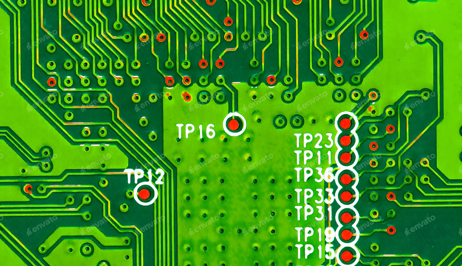
One of the most important steps in improving testability is placing well-sized, accessible test points on key nets. These include power rails, clock lines, reset signals, and data paths. Test points should generally be about 35 mils in diameter and spaced at least 100 mils apart to ensure compatibility with both manual probing and automated test equipment. It's important to avoid placing test points under components or in areas where probes cannot reach them, especially if using flying probe systems.
Component accessibility is another major concern. Parts should not be placed so closely together that test probes or inspection tools cannot reach them. A spacing of about 100 mils is typically sufficient for most manual and automated test setups. It's also helpful to maintain consistent IC orientation, as this simplifies inspection and reduces human error during validation.
Observability and controllability are core DFT principles. Observability means being able to measure what's happening inside your board, while controllability refers to the ability to influence or stimulate signals during testing. You can improve both by adding debug headers, jumpers, and even test pads for internal signals. Exposing reset lines, enable pins, and status LEDs can also provide valuable feedback when validating the board during development.
Another valuable strategy is partitioning your design into testable blocks. For example, power circuitry, analog front-ends, digital controllers, and communication interfaces can be laid out in such a way that each can be tested independently. This might involve using zero-ohm resistors or removable jumpers between sections, which allow one area to be powered and validated in isolation without interference from the rest of the system.
If your board contains high-speed signals, it's important to consider how testability intersects with signal integrity. Probes and stubs introduced by test points can act as impedance discontinuities, causing reflections or crosstalk. In such cases, use resistors or small series elements to protect sensitive nodes, or move test points slightly off the main transmission line to preserve integrity while still enabling access.
A Step-by-Step DFT Workflow for Beginners
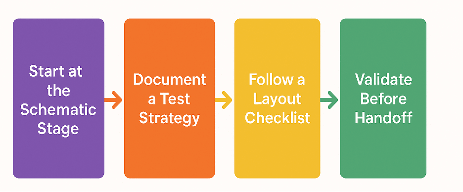
The best time to start thinking about testability is during the schematic phase. Identify which signals will need to be monitored or controlled, and build those test points, headers, and indicators directly into your design. From there, you should document a test strategy that outlines what needs to be verified, how it will be done, and what equipment or access is required.
During layout, pay close attention to spacing, pad size, and orientation. Use a checklist or consult with your manufacturing partner to confirm that your design is compatible with their test equipment. Don't wait until after your board is complete to validate testability. Use your ECAD tool's DFT analysis features or manual reviews to check that key points are accessible and properly spaced.
Before final handoff, share your test plan and DFT-related layout features with your fabricator or assembler. This collaborative step is often overlooked, but it ensures that your design aligns with their inspection and test capabilities, reducing the chance of costly changes after production begins.
Tips and Best Practices for Real-World DFT
Working with your manufacturer early in the process is one of the most effective ways to improve DFT. Ask them what test methods they support and what constraints their equipment may impose on test point size or placement. If you're designing for automated optical inspection, include fiducials and clear silkscreen markings to assist with camera alignment.
For boards with high-speed signals, consider including a test coupon for impedance testing or time domain reflectometry. If your board supports boundary scan, make sure the JTAG header is placed near the board edge for easy access and is documented in your schematic and layout notes.
Each of these steps may seem minor, but together they can mean the difference between a board that passes on the first try and one that requires extensive rework.
Final Thoughts

Testability is more than just a checklist item. It is a critical mindset that influences how your design performs, how easily it can be validated, and how confidently it moves from prototype to production. By applying Design for Testability principles early in the design process, you set the stage for smoother development, fewer surprises, and stronger product reliability.
Simple decisions like placing test points, isolating functional blocks, or preparing for environmental stress can have a major impact on manufacturing success and long-term performance. These are the habits that help engineers move beyond just making things work and toward building hardware that lasts.
Whether you are designing a board for a one-off prototype or for full-scale production, prioritizing testability will always give you an advantage. Make it part of your design workflow, collaborate closely with your manufacturer, and approach each project with validation in mind from the very beginning.
When your board is easier to test, it becomes easier to trust.