PCB Stackup Design Guidelines for Performance With OrCAD X
Key Takeaways
- A PCB stackup design is the arrangement and configuration of different PCB layers composed of conductive traces, insulating materials, and additional components.
- PCB Stackup design affects the performance, functionality, and reliability of your PCB. When designing a PCB stackup, there are several considerations to take into account, including layer count, signal integrity, plane decoupling, and material selection.
- Discussion of OrCAD X tools that aid in following good PCB stackup design guidelines.

Side and top view of a dense PCB stackup design.
A PCB stackup defines the order, thickness, and materials used for each layer in the PCB. Layers are either composed of signal traces or plane layers that provide power and ground. PCB stackup design affects the performance, functionality, and reliability of your PCB. It impacts signal integrity, power distribution, impedance control, and thermal capabilities. To follow good PCB stackup design guidelines, material selection, stacking order, and layer thickness should be carefully considered to meet design requirements.
PCB manufacturers often provide stackup design specifications that consider factors like impedance matching, controlled dielectric constants, and thermal dissipation. Engineers follow these PCB stackup design guidelines while considering the specific requirements of the circuit and the system in which the PCB will be used. Read on as we discuss PCB stackup design guidelines.
PCB Stackup Design Guidelines
When designing a PCB stackup, several important considerations must be made to ensure proper functionality, signal integrity, and manufacturability. First, we’ve highlighted guidelines concerning copper placement, from planes to traces.
|
PCB Stackup Design Guidelines for Copper: Traces, Planes, and Signals |
|
|
Layer Count |
|
|
Power and Ground Planes |
|
|
Plane Decoupling |
|
|
Signal Integrity |
|
|
EMI/EMC Considerations |
|
|
Signal Layer Ordering |
|
|
Impedance Controlled |
|
PCB Stackup Design Guidelines for Manufacturing and Material Selection
In addition to the actual placement of the copper, material selection and manufacturing constraints should also be considered when following PCB stackup design guidelines. Below, we've highlighted some important considerations.
|
PCB Stackup Design Guidelines: Material, Thermals and Manufacturing |
|
|
Thermal Considerations |
|
|
Manufacturing Constraints |
|
|
Material Selection |
|
Of course, specific PCB stackup design guidelines will vary depending on the project's specific requirements, such as the frequency of operation, environmental conditions, and industry standards. Consulting with an experienced PCB design company like Cadence can provide valuable insights and guidance to ensure you have the right PCB stackup design for your project.
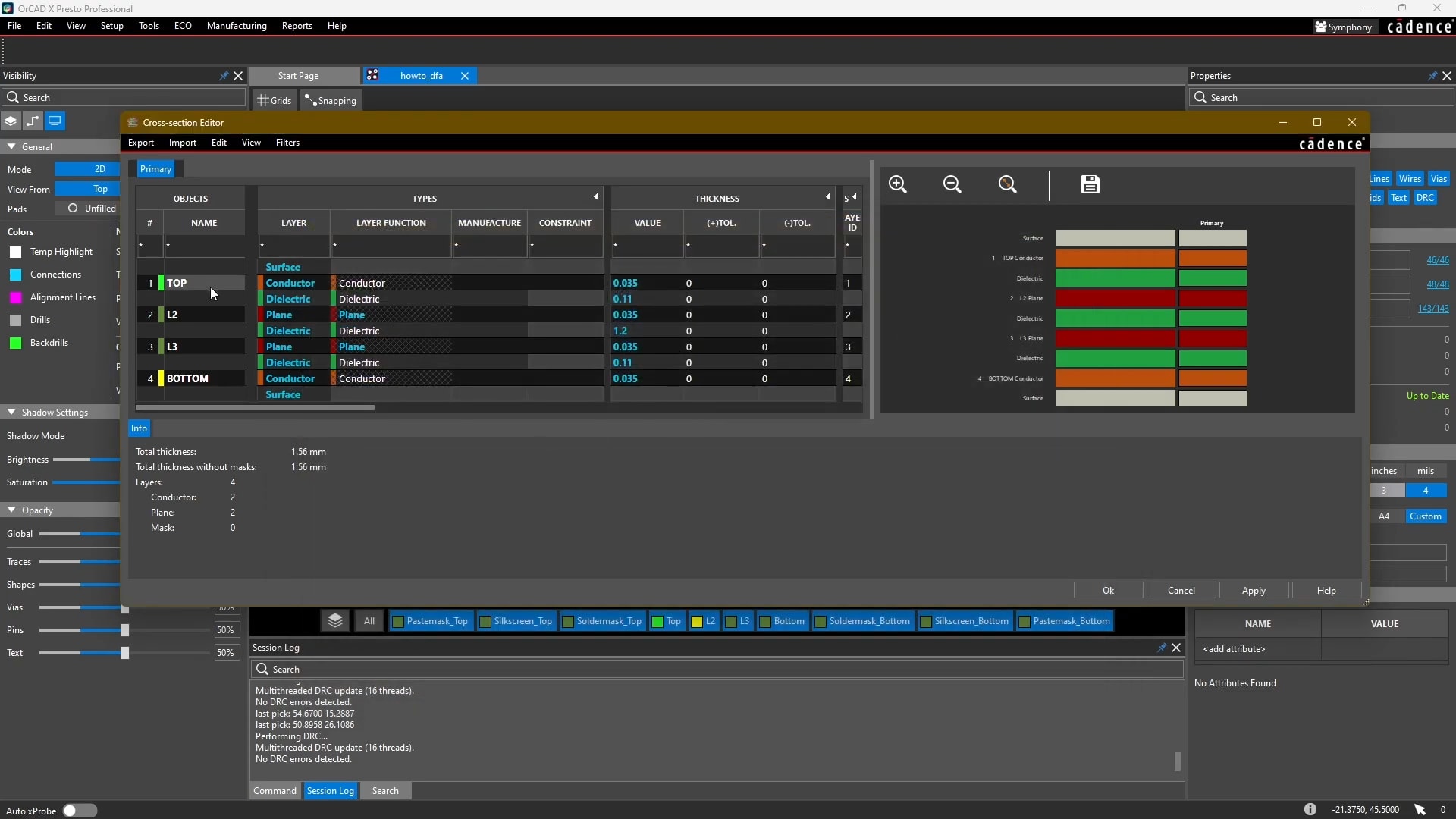
OrCAD X cross-section editor
OrCAD X Features for PCB Stackup Design
|
OrCAD X Feature |
How It Helps in Stackup Design |
|
|
|
|
|
|
|
Via Arrays |
|
|
|
|
Copper Polygon Shape Pour |
|
Mastering PCB stackup design guidelines is crucial for ensuring your PCB performs optimally with signal integrity, effective power distribution, and efficient thermal management. By leveraging OrCAD X, designers can streamline the stackup design process. To explore how Cadence can enhance your PCB design process, visit our PCB Design and Analysis Software page and learn more about OrCAD X.
Leading electronics providers rely on Cadence products to optimize power, space, and energy needs for a wide variety of market applications. To learn more about our innovative solutions, talk to our team of experts or subscribe to our YouTube channel.