The Design Rule Kit and Why You Might Want One
Others might be solving the same problems you are. Leverage the commonality so you can focus on your core solution.
A Design Rule Kit is a little like the Process Design Kit (PDK) used by chip manufacturers. The chip designers are very much beholden to the foundries that turn their tiny dreams into an electronic reality. As Printed Circuit Board design becomes more complex, a Design Rule Kit becomes all but inevitable. Instead of one set of rules based on possibly outdated IPC specs, we can go with a set of rules from any vendor who participates in the program.
We really do have it backwards. The PCB is designed and the artwork package is cleaned up in Valor (1). Cleanup includes a quick going over to see if all of the data is there and coherent. The artwork overlays reveal the usual DFM errors starting with text where it should not be and next, a request to add some text back in for regulatory and date coding purposes. It goes on. Global micro-editing or “etch compensation” will be the final assault on your precious artwork.
“If you only knew what we did to turn your Gerbers into a photo tool…”
So, these experts craft a more complete data set and the planner feeds it into the machinery on hand. Their formulas for the etch compensation will be calibrated to that specific equipment. Lasers are an exception. When it’s no longer a chemical etching process, the nominal values are just fine. In this way, the equipment throughout a plant will have a certain level of technology. They tend to specialize so as to carve out a niche for themselves.
Of course, they would be happy if you found their niche to your liking. More happily, they’ll share the recipe with us. Then the boards will be exactly what they can build without so many “technical questions” at the beginning of the fabrication cycle. That, of course, is the theory. Now let’s try to package all of these electronics in the tiny space allotted for them. It’s only a matter of which rules am I going to break? Bend, not break. There may have to be room for some emerging technology in your build. That’s progress.
Rules
Pushing the right boundary can get you into a decent outcome; while going over the edge in any aspect of the design will, by definition, be a problem. Some of the levers we control are:
-
Material types, stack-up
-
Controlled impedance definitions
-
Library (Min, Nom, Max)
-
Spacing rules
-
Physical limitations
-
Whatever sets it apart in the first place
It is this overarching set of fabrication and assembly constraints that define the costs that a product will extract through its manufacture. Whether that is a profitable number depends on what people will pay. (Hint: we’re cheap)
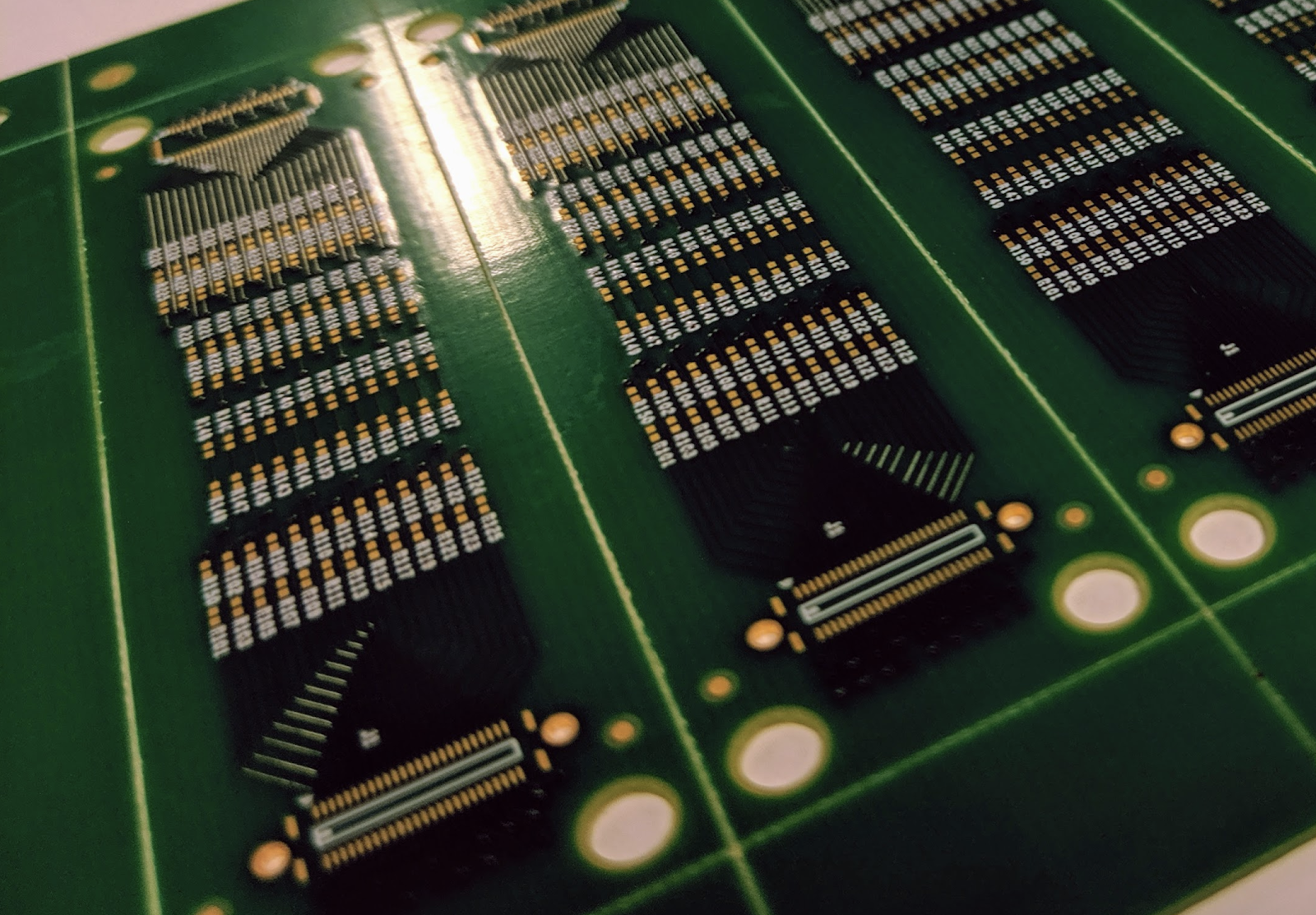
If you have a hot product on your hand and have to pass it on to an ODM, a “FloxConnix” type of company, they will have an associated PCB fabrication company on the job. This company will also be quite large with locations all around with varying levels of technology. Unless your company logo has a bite missing, the top tier fab line is for someone else. We’re somewhere down the food chain but their third best fab, assembly and test engineers are probably good enough.
Like anywhere else, you pay to play. It doesn’t matter who you are, Chromecast was built in Multek’s fifth and final tier. No stacked micro-vias for Chromecast; call it a 1+1+N+1+1 stack-up. There was a stagger of micro-vias on layer two and a micro-via to core-via stagger on layer 3 which only took me to 4 of 6 and I guess we were lucky to get that on a $35.00 price point for the whole dongle. Naturally, I started with the vias stacked but then had to do what we do. It’s just nice to have a menu right from the start.
Image credit: Author - maybe a ⅓ of the way to placement
Putting the data out front is exactly what the Design Rule Kit can do for you. Though most of us can memorize a long list of static rules of thumb regarding PCB layout, there are always opportunities to improve on that.
Time
There is no pause button in real life. Gradual improvement in the industry sneaks up on us until what we know is obsolete. Sitting still is moving backward so every facet of PCB layout moves ahead over time. Ahead is nominally defined as going towards smaller and smaller geometries.
Future proofing your library and design rules against the inevitable march of progress makes sense.
Future proofing your library and design rules against the inevitable march of progress makes sense. Having a continuum of design rules that run from the bare minimum to full-on NASA overkill boiled down to the price point and expected longevity is possible. It might even be necessary in a world with a supply chain that could pivot on a tweet. Call it agile fabrication shop engagement as a defense against the unknowable.
Place
Multisource agreements tend to create sub-classes of boards using similar technology. Different companies do similar computing tasks in their usual variety of form factors leading to the overlap of the typical boards in any market. Toys to gadgets to machines to robots, the various sectors have their own vision of a supply chain and an assembly line.
What may be mainstream in one location is too exotic to exist in another. Even when the differences are not that extreme, having a detailed technology roadmap built right into your layout software has obvious benefits. Stack those roadmaps up and see whose technology most aligns with your own.
Beyond technology, your procurement team is balancing cost, schedule, quality, relationships with your verticals, dependability, reliability, and even likability. There are a lot of variables to manage. Getting your printed circuit board designed and working in one pass makes it all worth it.
-
Valor or CAM350 or maybe some other Gerber editing tool is used to allow for their output to look like your input when it’s all done. Since we’re erasing the space between the lines, the air-gap is the actual limit of the line width battle. Different machinery will require slightly different starting numbers.