Fill form to unlock content
Error - something went wrong!
Fill Out The Form to Continue Reading
Thank you!
PCB Design Strategies: Optimizing Mixed Signal Circuit Designs
An Analog World is Where We Live. A Digital World Drives Our Data.
Right on the heels of the Power Distribution Network would be any analog blocks. If you do not go with minimum component spacing for the entire RF chain, then expect some blowback from the engineers. I will do that placement on a one-mil grid or even less because I expect a lot of scrutiny on analog placement.
Why? Simply put, because it's not digital. Digital circuitry translates to yes and no (it works well enough or it doesn't) while analog is a gray scale from zero to infinity where we're always chasing a fraction of dB of isolation or some other metric on a sliding scale. It's a different mindset and you have to prioritize analog circuits as much as possible.
Figure 1, as seen below shows an op amp in an 8-pin DIP package. It would have a feedback resistor as close as possible to two of the pins and a bypass capacitor between VCC and GND. There are two leads on the input side with polarity and one output pin. Any of those I/O pins could be enhanced with an RC filter or something similar.
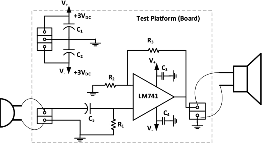
Figure 1. A mic, a speaker, a few terminals and an op amp with its constituent passive components; this is a core analog circuit. Aside from audio electronics, these types of amplifiers are common in current sense applications used on eval-boards. Image Credit: University of Bath
Every part would be on the top side and have leads going through the board. That's what analog meant when I got into this game. What once fit in a suitcase, now tags along in a back pocket and is completely wireless. The shrinkage of our electronic devices has been astonishing.
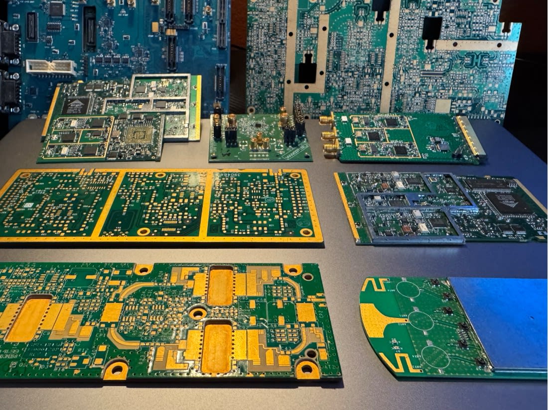
Figure 2. Half of my PCB curriculum was spent on analog design. That's good because more than half of my career was also spent on these things. Image Credit: Author
While antenna theory is still in effect, the means of transmitting signals has gone parallel for broadband network access. Analog signals are typically digitized then chopped up and sent over multiple frequencies to be assembled back into media on the user end. Multiple Input, Multiple Output (MIMO) radio sets are a common way of increasing bandwidth.
Shielding is inevitable when we're condensing lots of applications within an enclosed area. A large sector of the consumer goods industry falls into the multi-functional IoT devices where low power consumption and some form of wireless communications go hand in hand. I may not be battery operated but my life seems to be. Between my phone, laptop, camera and car, which one has better GPS?
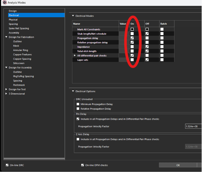
Figure 3. Fundamental to using the constraints is the Analysis Modes window. Right now, we are checking for relative propagation delay and differential pair integrity while setting aside any warnings regarding net schedule, impedance, layer sets, unrouted nets and minimum delay. You'll only see what is selected in the Modes options. In this view, we're only dealing with electrical constraints. Image Credit: Author
As the timeline progresses, the resonant frequencies of a few GHz made room for 60 GHz "WiGig" for close range applications. The 5 GHz radios are equivalent to ethernet speed while the 60 GHz bands are taking market share from the HDMI camp. It may be wise to implement these radios as modules that sit on their own substrate and also use the tiniest of components that would drive cost if implemented on a larger board.
So called Front End Modules are an industry of their own. The complex matching networks for the Multiple Input/Multiple Output (MIMO) radio schemes are packaged as a unit. They cater to any number of receive and transmit chains that are commonly used.
There's an industry around the notion of a Front End Module (FEM) where the typical matching networks for a MIMO radio are all on a single rectangular board that is mounted to a through hole or surface mount motherboard. This would streamline production by consolidating these component intensive circuits on a manageable component footprint. The board as a whole would not necessarily benefit from exotic material and the miniaturization that goes with RF circuit boards.
Ah, the Memories - Let's Double Up on the Data Rates
I would put memory down as a strong second place in the hierarchy of placement and routing. The most layout sensitive memory is the type that is using both the up and down swing of the clock to regulate the data rate.
Known as Double Data Rate (DDR) Dynamic Random Access Memory (DRAM), it has more going on than other types of memory, be that Serial Peripheral Interface (SPI), Embedded Multi-Media Card (eMMC) and so on, as those types are for storage rather than computing. The complexity of DDR manifests in numerous lanes of data and address buses along with a reference voltage supply and other esoteric nets.
DDR memory is segmented into several bytes, typically eight bits (nets) each with their own timing requirement within the byte lane and again with respect to other byte lanes but to a lesser extent. Two bytes form a so-called "word" for a total of 16 bits.
Four bytes equals two words or a "double word" equivalent to 32 bits and a "quad word" is good for 64 bits. It's all broken down for parallel processing to improve system performance. The end result is that we spend significant time generating match groups with potentially overlapping constraints. You're tuning lane to lane as well as within each lane.
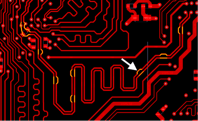
Figure 4. The yellow segments are telling us that we have exceeded the maximum uncoupled length with all of the phase matching bumps for the clock pair. My first move would be to use arcs instead of the diagonal bumps. We could also pull the jogs closer together so there is better coupling. If all that fails, we might see if the spec can be waived to allow what is on the board to stand. Image Credit: Author
Note that when dealing with length matching of the clock, it can be giving you DRC errors that tell you that it is both too long and too short. What that means is that the problem may not be with the clock but with other members of the bus with some being too long and some too short.
Always phase-match the clock pairs using best effort to center-cut the meter. This provides the greatest amount of leeway for the other traces in the bus to meet the target length. The individual traces must match both legs of the clock diff-pair to within spec. There's more latitude when the positive and negative traces are the same length.
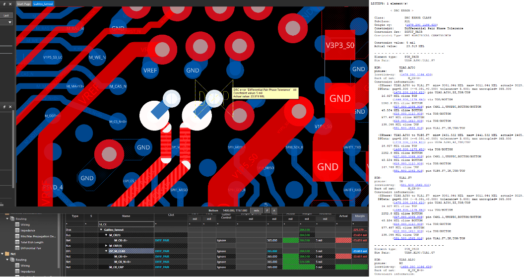
Figure 5. The phase tuning bumps were removed which cleared up the uncoupled length error. The result is that the negative side of the Clock diff-pair has to be lengthened by ~28 mils to recover the phase matching to within 5 mils. Image Credit: Author
The number of nets in a DDR memory bus is substantial, especially compared to the other types. A rule of thumb that helps setting up the constraints as that a chip with fewer data lines is apt to require a tightly controlled timing budget.
Meanwhile DDR generally has more slack especially between byte lanes with most of the effort going into length matching within individual lanes. As I pointed out above, those bytes can be combined into words where the number of members in each group doubles and doubles again until the requirements are met for high bandwidth memory.
So far, we have looked at components whose placement is determined by the mechanical considerations followed by decoupling capacitors, crystals, RF chains and memory. The fourth pillar of important placement items is those that are especially sensitive to outside interference.
While WiFi, Bluetooth, GPS, NFC and others fall under the RF domain, there are other types of sensors that require more board space than their size would suggest. Microphones, pressure gauges, Lidar sensors, compasses and other sundry items require a wide berth that could very well extend through the entire board as well as outward on the surface.
Figure 6. Now the clock net is fully compliant within the pair and with all of the single ended memory lines that use the clock in question. The uncoupled length was washed out with the rounded "speed bumps". While I'm straying from the theme of placement here, you want to be aware of critical nets as you do your placement. Image Credit: Author
The device might want a quiet corner of the board. It may require its own power supply which should be in the vicinity but out of the line of fire. Special treatment may include provisions for pulling heat away from the device. Power may come in on more than one layer so that the shapes occupy a narrow corridor that doesn't get corrupted by outside interference. Placement time is also fanout and route planning time.
The engineers on the project may not have the wherewithal or time to look at a placement in the absence of the rest of the story. If you're doing the placement of the critical analog parts properly, then the routing should be straightforward.
I would normally make those connections and even pour copper around them before sharing with the team. At least, they can see what you have only visualized. I'd go so far as to populate ground vias along the path so that the space is claimed and they can see that you want what they want even before they have a chance to say so.
Figure 7. When the official plan is to route the DDR on an outer layer, space must be set aside for that purpose as you can see how it expands from the number of traces and the required spacing. This along with any analog connections are high priority as routing ultimately drives placement in these cases. Image Credit: Author
One of the best things I ever heard from the EE was that he would make a list of things he wanted from the previous submission only to find that those things were addressed with another iteration before he could compile the requests and send them to me. Push out your work early and often so that you don't get ahead of yourself. Try to think ahead of where they would go with that version and take initiative. You will earn their respect by being proactive. At some point, I would even tape the board out so I can clear up any roadblocks that may be lurking in the design.
Missed Part 1 and 2?
Read Part One Here: Designing for High-Pin Count Devices
Read Part Two Here: High-Density Interconnect (HDI) Techniques