My Favorite Component - How to Succeed With Switch Mode Power Supplies.
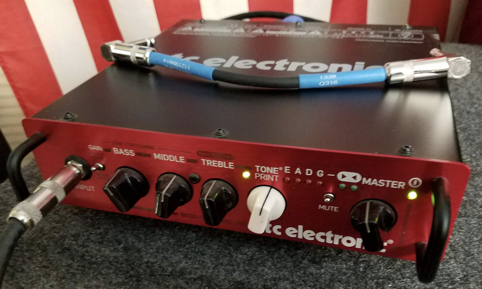
Image credit: Author - Replacing an amplifier with one that weighs a tenth of a traditional solid state amp.
It started long ago, or at least long ago in terms of internet time. Going mobile had several ramifications for the companies that wanted to be in the hardware business. Of course, radio technology had to be developed to cut the cord. That’s a given. Disconnecting also meant bringing your own power plant with you. A solar generator stores thermal energy during the day and uses it to light up the night. The mobile devices use an umbilical or a capacitive means of accruing that power while we sleep. The cycle continues.
The limitation of the pocket or lap sized gizmo is the number of Amp-Hours its battery can store. We know that the more battery cells you can pack together, the more “oxygen” the various devices that make up the product can breathe. We know this since every generation of the product has a bigger battery and a smaller printed circuit board. That is progress. Another thing progress has going for it is that we will add new and improved features. Those new features almost always involve some new circuitry to run the new software, maybe even a custom ASIC to bring to life.
That is to say that our job in the mobile space is about doing more with less. High-Density Interconnect (HDI) techniques can help us shrink down the circuit. This is the continuing game changer. Smaller components and PCB features may cost a bit more to implement, but that is a better alternative to coming in second in a two-horse race. We’re managing increased thermal and RF coexistence problems through simulation, verification, and reiteration. Product development has never been easy. We’re are getting better at it though. With the rise of the Makers movement and 3D printing, the number of contestants on the field will be a lot more than two. No good idea goes unemulated.
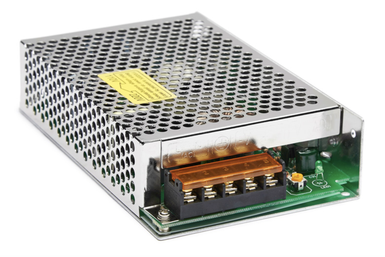
Image credit: Makerlab electronics - commonly used for AC (wall socket) to DC (internal power) conversion.
What’s the secret sauce for mobility? Not wasting a milliamp-hour of that precious battery power. In a marketing breakthrough, we can start with 2000 milliamp-hours instead of just two amp-hours. The point is to make them all count. This is where my favorite circuit comes in. The switch mode power supply (SMPS)!. These are DC/DC converters that supply a precise amount of dedicated power to a component that may be sensitive to ripple or other fluctuations to its voltage-in pin(s). The one shown above with its own Faraday cage is on the large size. Compared to linear regulators, the packages are much smaller though offset by the size of the inductor used with these devices. The smallest ones I’ve seen are 4-pin BGAs on 0.4 mm centers.

Image credit: eBay - much larger than the actual size of around 1 mm square.
The real two-fold gift of the SMPS is efficiency. It does a better job at converting one voltage to another - swapping current for amperage - while also generating less heat. Creating heat is a feature of linear regulators. They come with a mounting hole so they can be bolted to the chassis or a heat sink. That is your power just bleeding off as heat into the atmosphere. Most components will last longer if not subjected to repeated temperature excursions. Keeping the temperature relatively constant is one way to prevent the end of life for a product. We have to do better and we have a plan.
But not so fast! There is a catch. What an SMPS makes instead of heat is switching noise. Shouldn’t be a surprise given the name is Switch Mode. The device works by quickly charging an inductive coil then switching off while the coil, along with a small capacitor, release that burst over a longer period of time. As the LC pair have about run down, the device opens the gate again and refills the coil once again. And again and again to create a steady state DC signal out of one of the most bipolar sources imaginable. Yes, I know; you and Han Solo both can imagine “a lot”. Just know that they are aggressors and protect your victim circuits accordingly.
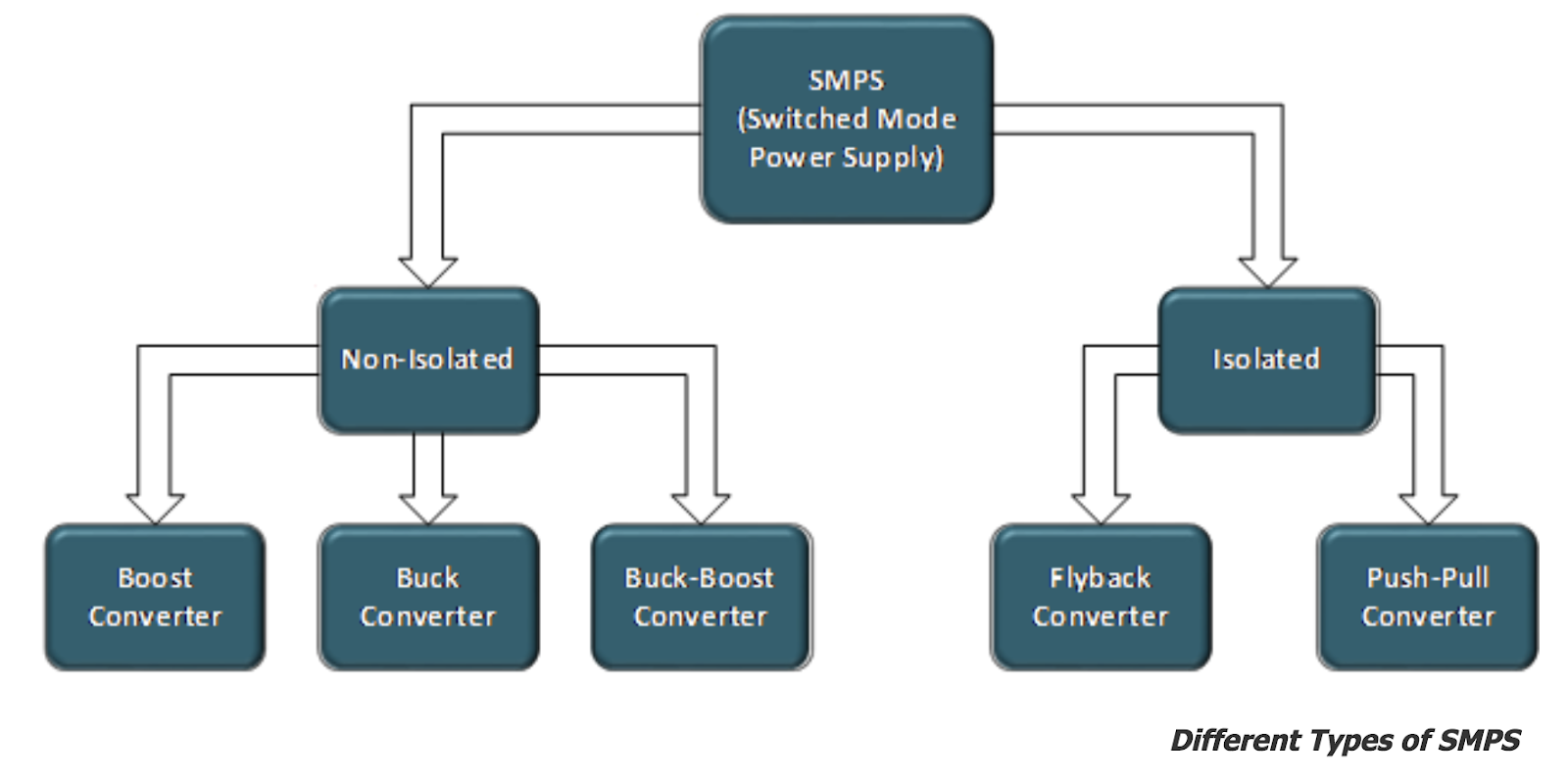
Image credit: Engineers Garage
Attenuating that residual noise takes a little effort on the part of the PCB Designer. Everyone who has to look at data sheets knows that we should keep the inductive loops small with tight capacitor placement and routing techniques. The current within the inductor is another inseparable part of the equation. The shortest and widest path is between the power supply output pin and the inductor so that the power can keep up with the switching speeds of the information, whatever form that may take. The mechanism behind this is also the underpinnings of Class D amplifiers which make wonderful electric bass guitar rigs.
So, let’s get into why this is my favorite part.
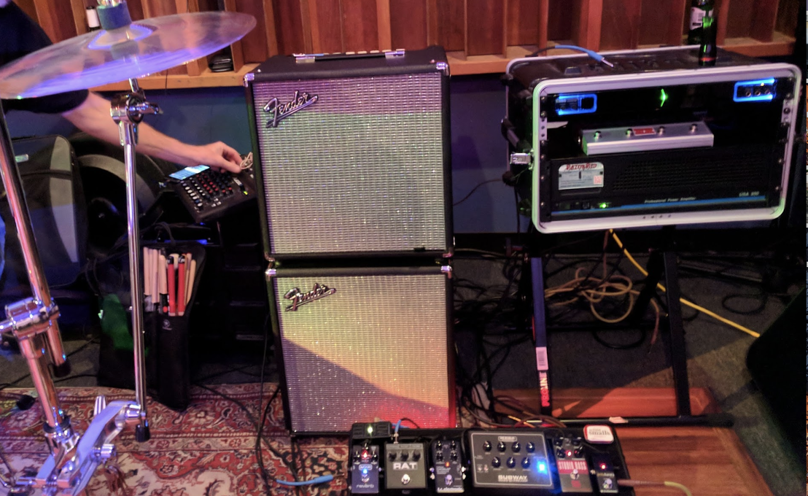
Image credit: Author -- Switch mode amplification.
The amplifier on the right takes up three “rack units” and weighs almost 40 pounds. It is more cumbersome because the weight is way off center with the heat sink off to the side of the unit. Buying this vintage equipment today would be really cheap. I can say that this equipment has been lugged around all over for more than 20 years but has never been lugged to a repair shop. In its day, it was touted as the lighter, more durable technology over vacuum tubes. Vacuum tube technology is still prized by many despite their delicate nature, their noisy operation (hum) and inherent inefficiency.
Unlike vacuum tubes, the mini stack on the left was also a low investment - but then I voided the warrantees by upgrading to neodymium magnet equipped drivers. They weigh a fraction of their ferrous counterparts. Sometimes, you have to crack something open just to see what the printed circuit boards look like. They look just fine. Having two separate amplifiers increases the chances of getting through a show without a catastrophic loss of low notes. The entire stack weighs less than the racked amp.
The newer, better Class D switching type bass head goes into the pocket of the guitar backpack with room for the cord. Parasitic losses are very low with efficiency ratings above 90% being common. The title image is one such product.
Power Management Integrated Circuit (PMIC)
In addition to being sold as single-gate devices, there are packages full of noisy little power supplies available. Normally, you would want to put the SMPS near the load. By the way, the device that is being driven could have a voltage requirement above or below the Vin. A “buck-boost” or buck-converter can deliver outputs above or below the main voltage so that every chip gets what it needs. The so-called System On a Chip (SOC) will have many different voltage requirements. Every interface, every neighborhood on the whole ball map of 1000+ pins will get its own power supply.
Instead of twenty little power supplies, the monolithic Power Management Integrated Circuit (PMIC) gathers them up into a ball grid array package. This innovation puts the layout person in a bit of a bind. Remember the part about placing the inductor and cap close to the output pin? The pins are much too close together to have a shot at that. The layout is about a compromise where all of the constituents feel the pain.
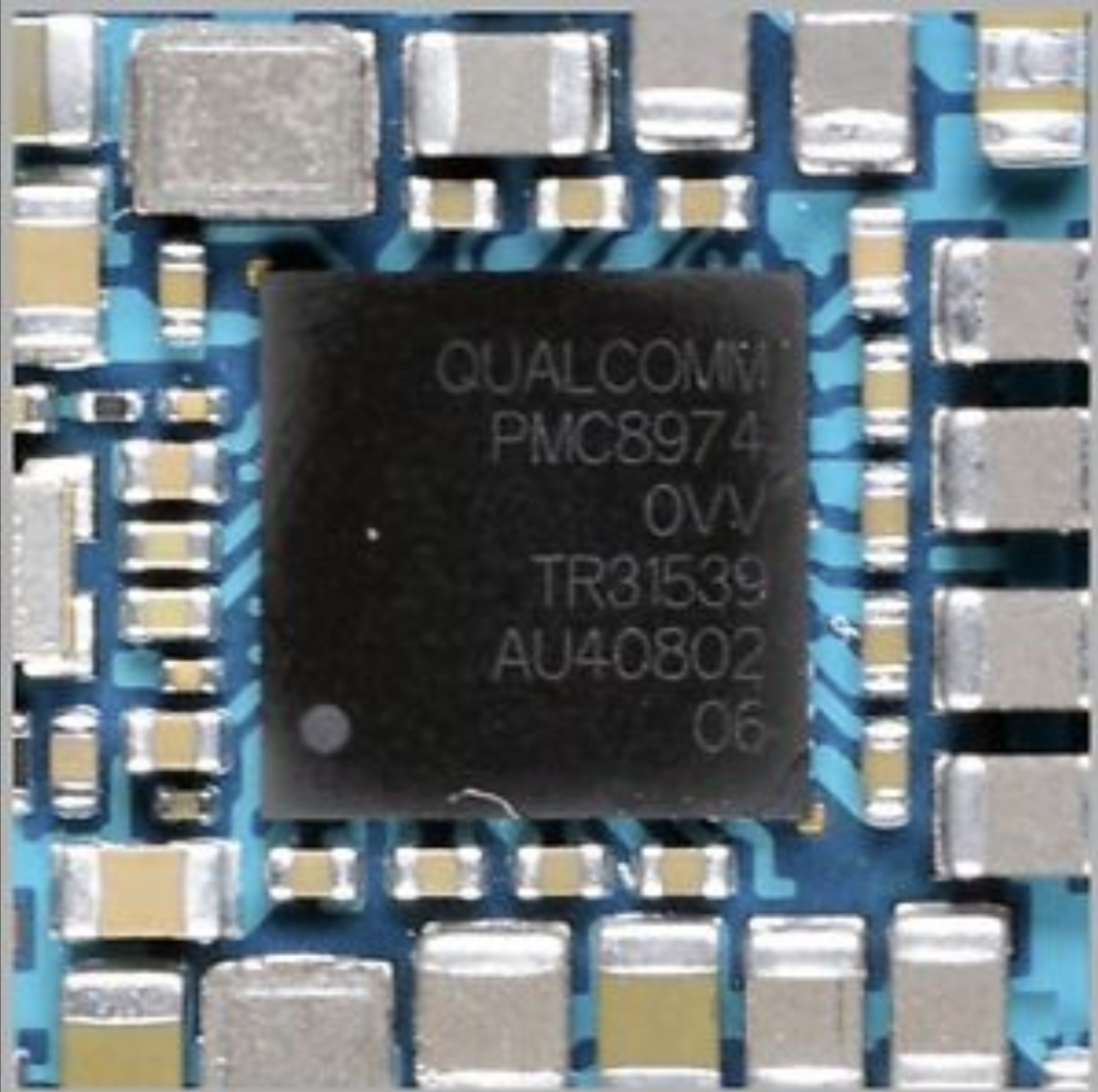
Image Credit: eBay - PMIC, equivalent to 12 SMPS devices
My first impulse was to at least get all of the input and output caps near the pins. The back side of the BGA device is where we usually place our decoupling capacitors for best effect. That notion still holds true on the voltage input pins. The PMICs that I’ve seen generally have the Vout pins around the edges of the device. Place all of the inductors in a frame around the device. The routing would be in the form of shapes radiating out from the PMIC to the inductor pins. The output bypass caps are essentially shoe-horned in between. There will be clocks between the SOC and the PMIC and they will be hated by every other thing on the board because they are bad and noisy neighbors.
Low Drop Out Regulators
Low Drop Out regulators are linear regulators that are small in size and are also paired up with an inductor/capacitor combo plus a little sense circuit. While they can deliver a positive or negative voltage, the definition of low drop out is that the input voltage has to be pretty close to the intended output voltage of these devices. If your supply voltage is 12V and the load device is looking for 3.3V, this would not be a solution. Contrast to an SMPS that would operate primarily in the off mode so as to average 3.3V over time.
Finally
Whether you are driven by mobility or simply increasing the efficiency of your plugged-in products, switch mode power supplies can be a factor while ensuring reliability. A few design guidelines from your vendor will steer you to a successful implementation. It might be time to switch.