CoDesign and Outsourcing PCB Design
Looking at a spread of components on a printed circuit board without any connections completed can be intimidating. Where does one start? That question was too much to answer for one of my colleagues back in the day. I guess you could say that he was a deer in the headlights, unable to move forward after placing both sides of the board.
The board in question was called the Integrated Module meant to replace a collection of five boards with various functions. It was a 10-layer, double-sided HDI board in a time before HDI was a common thing. It was the most complex board for the company up to that point. One of the evergreen rules of a startup is that you're going to do whatever you have to do in order to succeed.

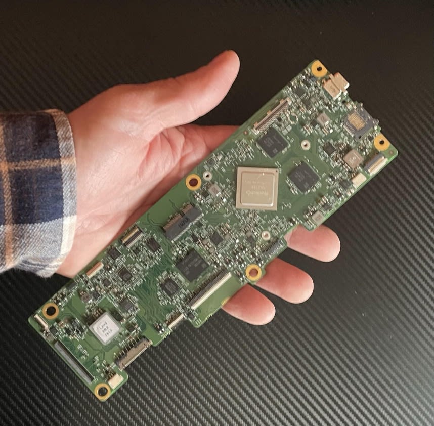
Figure 1. Main Logic Board for a Samsung Chromebook Pro from around 2018. A six layer reference board using 1-N-1+ stack-up technology. We basically get a second layer of micro-vias from layer 2 to layer 3 using only two lamination cycles. The 45 degree twist for the CPU helped the DDR length matching and made it look cool on the monitor. Show me an edge and I'll show you a connector! The diagonal orientation gave us a longer runway on each side. The sides facing the two memory chips use topside routing. Making the connections would be easy compared to tuning the data and address groups. It's nice to have multiple layers in play providing immunity for each lane.
Keeping Co-Design on Track in the Early Stages of Routing
The lead Engineer came to me and asked if I could help out. We worked out a plan where I showed up at 4:00 am and worked until 1:00 when Robert would come in and work 'till 10 pm. My part was layers 6-10 while he covered the top 5. Understand that the two of us and others came out of a team that did nothing but single-layer RF amplifier boards with a solid aluminum pallet as the second layer.
What do you do? Maybe give the auto-router a chance to connect the ground pins with a microvia-in-pad to the adjacent layer. Take a look at the results as a sanity check. Improve the fanout manually where it went astray. Just by fanning out the ground net, you have approximately 20% of your pins hooked up. Get a snack and mull over the next step with the voltage regulators while reusing every possible circuit as inspiration. That was my plan, I'm not above using shortcuts to get me to the next refill of my coffee.
Back to work. Connect the RF traces that could be done on the surface layer routing from point to point. Plan for the ground pour and shepherd vias that will be used to shield the analog traces as well as surround the RFIC. Take that space then try to preserve the buffer area as much as possible. Coexistence doesn't happen by chance.
Bring in the power on traces that are just thick enough to do the job without any excessive radiation. Even narrower spurs will extend towards the designated capacitors and their pins. The power delivery network was courtesy of Occam's razor while feeding fields of pins. In some cases, such as RF, less is more.

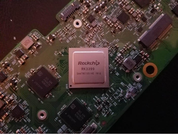
Figure 2. The Rockchip RK3399 "gets it" as far as the power delivery is concerned. The ball map has two power pins next to two ground pins. You can join the power pins through a single via, same with the ground and then drop a SMD 0201 capacitor between those two vias on the far side of the board. The chip has this arrangement over and over which makes placing the decoupling caps simpler. The DDR is pretty decent too with almost all of the data and address pins on the outer two rows for via-less routing of most of the two DDR memory chips. The Rockchip is a 17 by 17 mm package with 0.4 mm pitch.
The "last mile" of the power domain really was one of the tricky areas. We had to work out the star-routing to the power pins where a single cap is responsible for more than one power pin while three caps are dedicated to a single pin. Optimizing the power to the analog devices means using the least amount of copper that will get the job done.
That kind of specificity was difficult to capture. I got to learn all about net scheduling so I could drive the rats nest to maintain a line between the designated cap and power pin. To keep track of the plan, the highlight command was used not for the net but down to the pin level, matching the pin on the capacitor to the one on the RF amplifier.
The color code meant that we both knew the routing intentions. The schematic noted the associations and served as the source for this information including a power tree that diagrammed the grid by domain and showed how many milliamps to deliver to each pin. From there, the width of the copper gets calculated on the famous IPC chart that was already an old friend back in the 1990s!

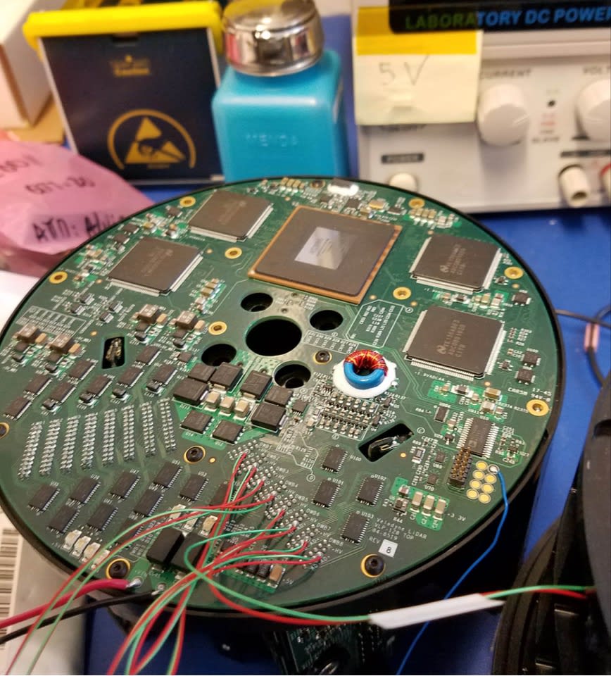
Figure 3. This 12 layer PTH board served as proof that via in pad using through-hole vias is a bad idea. It took a redesign clearing out all of the connections for the FPGA at the top of the board. The fan-out retained the through hole vias while space was allocated for the capacitors by sharing vias between the DC pins.
Now, with power squared away, lets get on those non-critical connections that could be done on the designated layers. Finally, there were several nets that reached both sides so when everything on layers 6-10 was good, I started dropping vias where they were required - letting Robert take it from there.
There may have been a little more back and forth between shifts but, working that way, we got to the finish line. It might have been nice to use partitions; they work by area, not layers. This was the late '90s so that wasn't an option.
Serial Or Parallel PCB Design Flow?
No matter the decade, teamwork isn't quite as efficient as a solo effort but it does compress the timeline. I've used the same method with service bureaus over and over since then. I've also been the swing-shift consultant showing up at 4:00pm. There is value in keeping the vendor hemmed into a specific area. A section within a shield or an area that uses high voltage design considerations might be farmed out to a service bureau.
This is just my opinion here, part of which comes out of this early work sharing experience. Keeping the board whole and working on it round the clock is more efficient than breaking the board up into two or more pieces. It could depend on the size of the board though.
While a partition is checked out, the owner of the rest of the board has to manage that boundary with care. Reinserting the new circuit for the old can be time consuming if the old stuff isn't properly cleared out. I prefer serial design to parallel for the types of boards I've done. Parallel design might work better if all of the designers are under one roof and on the same shift.
The HDI Decision Guide
There was always a through-hole solution available until the chips went mobile and shrank below the 0.65 mm pitch down to 0.5mm and further with each generation. The 0.65 mm devices are the last node that could be supported with normal vias. From there on, we use micro-via-in-pad techniques.
The 0.5 millimeter node is interesting. Just like silicon is measured in nanometer gate size, IC packages are marketed by their pin pitch. Point five millimeter puts you at the crossroads of routing a trace between the vias and having to dig deeper into the board using the Z-axis to escape the package. Welcome to the HDI barrier. At the root, the problem is the good old via.

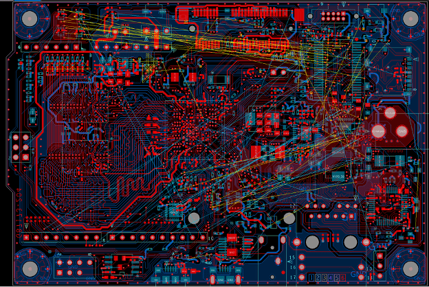
Figure 4. The fanout is complete and the critical nets are routed along with most of the power domains - particularly for the primary components where the tough compromises are made. The guideline for doing the remaining routing is to stay out of the way of the existing circuits that came before. This is a point where you can take a good weekend off and let the team carry the ball.
Staying a Step Ahead of the DFM Monster
PCB fabricators are "disinclined" (severe understatement) to give you a plated through hole within the surface mount pads. When they do it anyway, the assembly house is likely to register a complaint for yield issues during reflow soldering. Turning a through-via into a solderable surface is harder than giving you sequential lamination. Combine that with stacking micro-vias and the real estate cost of a via goes away until we get to the 0.35 mm node.
If you're wondering, we move to soldermask defined lands anywhere below 0.4 mm and even that one is debatable. About 60 designers who applied for a job at Google know what I'm talking about. Interviews came in waves so I was ready with standardized questions. It felt like a huge responsibility to be honest.
Where were we? Normal soldermask limits are enhanced with laser defined lands. Laser beams don't get dull or lose their strength over time but they do take some time. When it comes to silkscreen, it's still nice to have a laser printer so the little text can be read under a microscope. These precision operations cost more than screen printing would. These decisions will have to be made in concrete up front and take the form of a statement of work. The SOW drives the action along with the PO. One of the norms of working with an outside vendor is that you have your requirements well defined. They will accept your potential revision while adding an ECO fee. Ouch!
By definition, HDI will give rise to more congested boards where the silk screen will not be able to identify every component. The first element to go is the component outline when the space between parts doesn't support it. Then, the reference designators can be strategically eliminated where small parts are clustered. The thing we want most to preserve is the polarity marking for diodes, and similar safety information. Boards or assemblies too small to mark could use the bag-and-tag inventory method.
Beyond the artwork, the deliverables on the Design For Manufacturing front include:
- Drawings with notes that describe the finished board in both the bare and assembled state.
- Include a table with stack-up information weighed against impedance callouts, giving purpose and meaning to the layers and line widths.
- XY coordinates for placement of components and test points
- Netlist and Bill of Materials
- Some ODM's may ask for the ECAD database. Say no or go to File > Properties and lock the design with a password and permission to view only.
Build Confidence in the Vendor With Small Victories
Instead of doing non-metal work yourself, it is something that can be outsourced. I have no problem sharing the housekeeping work with a contractor. The fab drawing may need dimensions or other details. The assembly drawing and/or silkscreen could be organized ahead of a placement review. Shed a few of these mundane tasks as an ice breaker before cutting them loose with the general purpose routing.
Having a PCB Designer in-house is preferable if you have the infrastructure. Quite likely, it's a remote situation out of necessity. My key vendor has a local bureau here in Silicon Valley but also the overnight team working their normal day-shifts in Taiwan.
Happy Hour - A Stand-up Meeting Before Going Home Every Day
On day one, there is a full-on PowerPoint slide show with a few slides enumerating the design goals. Every weekday morning, the board comes back from the after-hours team and we review their progress while they're at home. We may or may not have created a partition for the local bureau to work on during the day.
Either way, before going home, we would add more screen caps and instructions to the PowerPoint. The afternoon hand-off could be the only time we could read in a new netlist. We gave them the whole board to work on at night and on weekends. Unless you have a hierarchical schematic, the logic is frozen while the layout is partitioned. When "happy hour" came, we consolidated the board and imported new logic, doing placement if necessary. People with schematic improvements had to wait for that window or be there with me at 7:00 am. That's one of the big strikes against partitions.
Every morning was like Christmas. Open it up and find out what you got. Compare what came back to what was requested and do any course correcting with more slides. When the service bureau takes over at the end of the day, there will be certain layers turned on, nets highlighted, and ratsnest enabled. That's their hill to climb. These visible clues are things that can be given daily, even if no other work was completed in-house, like on Christmas.
Managing Expectations: Garbage In = Garbage Out So Be Precise on the Requirements
The expectations will be as clear as we can make them. Even then, we might get a laugh at the results that come back the next morning. Sometimes, that would define a new PowerPoint slide and other times it would be giving a refresher on an older course correction. When it's the second thing, it actually validates why I would use a slide show to document the details of a design that employed more than one designer.
The first thing you have to do for outsourcing is the non-disclosure agreement (NDA) followed by setting up a purchase order for so many hours on demand. You start making phone calls and sending emails when the job in front of you has more content than the calendar provides. We do not judge by the color of the mask, only the content and the calendar. It's good to have that help on tap before you need it. Stay ready, my friends.