First Things First- Getting Your PCB Layout Off to a Good Start
First Things First- Getting Your PCB Layout Off to a Good Start
We've all been there, or we will be someday. A new concept has emerged and, the team is given a chance to own that niche. To save time, we're going to leverage an existing design. Yep, the good old design reuse scenario. The goal is cutting down on effort by sticking to a proven board outline, perhaps with an exception for a new connector. The reality that we're going to pack ten pounds of potatoes into a five-pound bag.
“A new design, whether it is an original or a new twist on an old favorite, needs a good foundation.”
Overcrowding aside, dropping a new or revised circuit into a preset form factor will occasionally be more effort than building a new chassis around the electronics. Compare it to building a new house out in the country to rehabilitating an old one in town. The first step I take is a survey of the design rules. Going over density metrics of the previous iteration and noting things like pin-count from before and after the net-list data from the new schematic is loaded will give you a good idea of what's ahead. The number of pins per unit of area will be the technology driver.
Demolition precedes construction
You will also have to take notice of the number of opens and shorts as well as any missing footprints that the net-list caused. The first real action on the layout is to remove items that are causing design-rule violations (shorts). This is not a time to be sentimental about a beautiful river of matching traces that go to the old memory. That memory is gone, and the new one isn't going to need the same routing. The well-crafted shapes that defined the old RF path and all of its ground vias are in the way. Trying to maintain the routing while the components are in flux is the road to repetitive stress injuries.
All is not lost.
By carefully removing trace segments around a device and then building a selection set that includes the part, the fan-out and the family of parts for that device, you can transplant the entire thing. For your guru (small g) mind trick, move the group of parts by an established amount in the X and/or Y dimensions. The trick is to know precisely how far and in what direction you moved the family. That way, when you find a layer of stuff that should also have moved, you know the delta for that piece of the puzzle. Of course, you want to save your data before trying a mega-move.
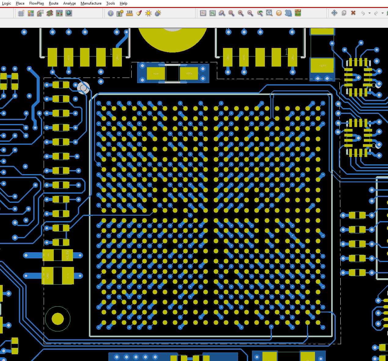
Figure 1 - We want to keep the fan-out and the passive placement.
Here is a walkthrough of a situation where a device has to move or become a reuse candidate. Figure 1 shows the device we want to ‘cut’. Everything inside the phantom line must go! That would be the device plus the column of parts to the left-hand side.
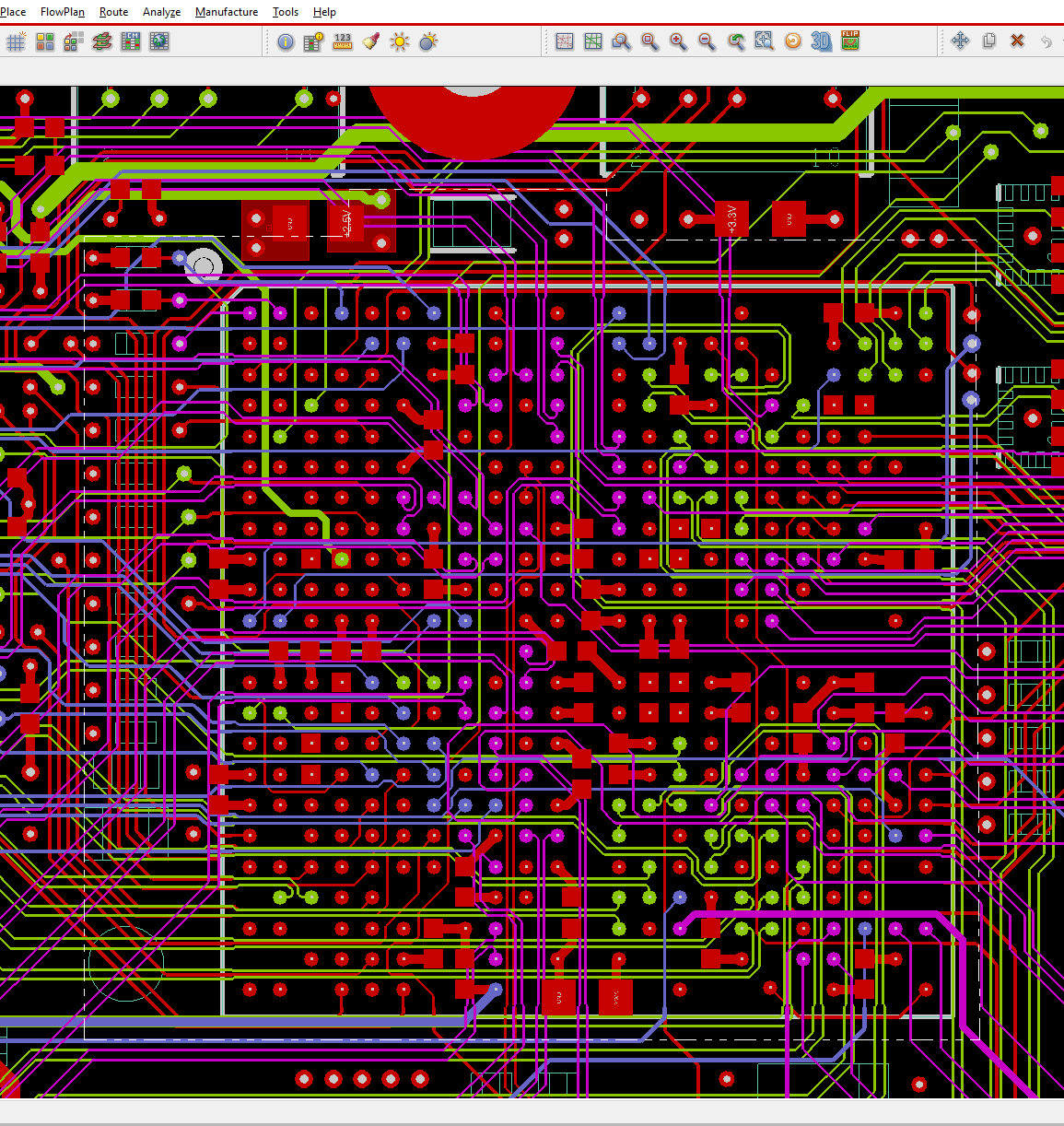
Figure 2 - ... but there is too much going on below the surface.
The scary part is that there is a mass of connections. The rational part is that you can take them a layer at a time and remove all of the trace segments that cross the imaginary line. Or, you can preview each layer and then take your segments out in four easy cuts around the perimeter.

Figure 3 - The device is ready to fly.
That’s what I did, and now the path is clear to grab this entire device for relocation. The leftover traces are in the same order and on the same layer as it was from the start so if the new location is reasonably close, the connections should go right back together. The power domains were not considered here but reshaping the copper to the new topology involves using the highlight command and creative polygons.
(Re)calibrating the Design Rules
Once the big chip floor-planning concept is approved, you should be able to flesh out the density level. IPC recognizes three levels and has design rules for the minimum, nominal and maximum sizes. The bigger pads act to give each part more space and also help manage the junction temperatures with their generous pad dimensions. This is the path to higher reliability.
The big pads also elicit complaints from the assembly line as they do not do as good of a job of keeping the components in perfect alignment through the solder reflow process. Everything is possible, but it comes at a price. In any case, never mix different density footprints on the same board. Two solder profile targets for the same part will ensure that at least some if not all of the solder joints will be challenged.
Stack-up verification
We now have our old board with a new parts mix and connection scheme. Time to validate the old stack-up. That part is easy. If you can fan-out the most convoluted device with routing channels to spare, you should be good to go. If there is no room for improvement or worse, the signals cannot escape cleanly, that is a sign of trouble.
This early in the design, it is unlikely to be the last time we hear from the schematic capture team. Most solutions to problems require more rather than less circuitry. We can not fix a problem until we know it exists. It is thus, natural to incorporate mid-stream improvements over the course of the layout. Anticipate this fact and try to leave a little slack in the placement here and there.
Green field approach
Maybe we are going to build that metaphorical house in the country. An all-new board outline indicates an all-new product outline. Expect a new mounting hole at some point. What may start out as a generous area for the board becomes hemmed in with package keep-outs and shields. The connector grew. Again. The gist is that the PCB is evolving on two fronts; physical and electrical. Everyone on the team starts with a general but hazy idea of what the finished widget looks like. We resolve on the final form with iterations - until the final day in some cases.
Setting the co-development aside, we get to the point where all of the components are on the board. The fan-out study has given us confidence in the old stack-up or has given us a new stack-up but either way, we made it to the first scheduling gate.
Placement.
Now is the time for high-level simulations of critical circuits. Defining the risky elements into three buckets for high speed, broadband, and power integrity lets us get ahead of the game with virtual iterations before any copper is etched. Connect all of the “special” nets and let the SI/PI experts dig into it. This early-stage of the design creates uncertainty which compels us to use the available technology to gain performance insights into your design. Simulation is easily one of the most critical force multipliers in our bag of tricks.
An adage from the restaurant business is applicable here. “Time to lean is time to clean.” Get the little things done between the rushes.
While we scrub for the simulations, it’s a good time to get ahead of the silkscreen, assembly sub-panel, and any of the various deliverables. It is likely that 10% of the parts will move and that those reference designators will have to be aligned again by the time the board is completed. That means that the other 90% does not need attention at the critical tape-out time. I’m guilty of focussing on the metal layers early on, so this note is for me too. Wise use of downtime over the course of the layout is another success enabler.
Going the distance
A new design, whether it is an original or a new twist on an old favorite, needs a good foundation. That foundation is based on getting your mind wrapped around the design requirements and crystalizing those requirements as electrical constraints and mechanical criteria. Placement that enables those practices evolves out of fan-out studies that reveal the pain points. It comes down to seat time with the layout. The most complex PCB ever designed started with one stroke. Then another...
Start with cleaning up the old artifacts and continue the housekeeping so the back of the schedule is not a Design Rule Check nightmare. Time management and a focus on capturing the design intent (rules) as part of the placement phase will put you, or the autorouter, in a good position to solve the rest of the puzzle. Effort up front is paid back along the way and paid with interest the next time the hood is opened. A good start does not guarantee a good finish but a poor start doesn’t have a chance. Choose wisely and we’ll see you at the end.