Designing Reliable PCBs for Space Applications
Key Takeaways
- Use high dielectric strength materials and techniques like via stitching and conformal coatings to handle high voltage in vacuum conditions.
- Employ high-frequency laminates, controlled impedance traces, and differential pair routing for reliable data transmission.
- Choose space-grade materials such as polyimide, ceramics, and high-Tg FR-4 to withstand extreme temperatures.
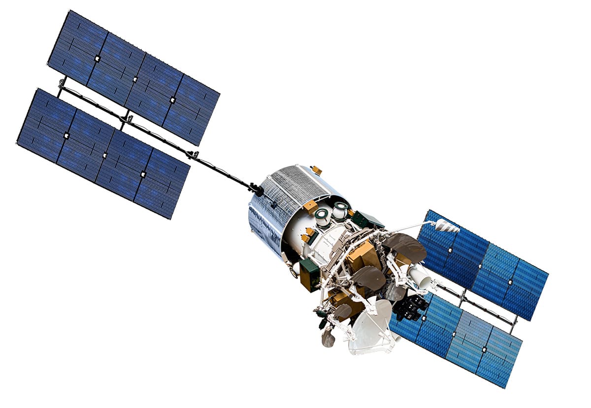
PCB for space applications includes satellites, rovers, and landers, space telescopes, space probes, and launch vehicles.
Designing PCBs for space applications involves addressing high voltage, high speed, RF, and EMI challenges to ensure reliability and performance in harsh environments. These applications include satellites, rovers, and landers, space telescopes, space probes, launch vehicles, and any other PCB that must withstand hard space environments. Here’s how these factors come into play.
PCB For Space Application Elements
|
Factor |
Description |
Design Techniques |
|
High Voltage |
Essential for powering components in communication satellites and scientific instruments. Requires handling without breakdown in vacuum conditions. |
|
|
High Speed |
Critical for data transmission and processing in space probes and rovers. Must maintain signal integrity to prevent data corruption. |
|
|
Radio Frequency (RF) |
Vital for RF communication in satellites and remote sensing probes. Ensures efficient transmission and reception of RF signals. |
|
|
Reinforcement Materials |
Used to enhance PCB durability and performance under space conditions. |
|
|
Design Complexity |
Complexity varies based on application and performance requirements. |
|
Regulatory Bodies for Space Application PCBs
When designing PCBs for space applications, it's best to consult the appropriate regulatory bodies for your intended use. For example, the NASA PCB Working Group (PCB WG) provides expertise in printed circuit board (PCB) technology assessment and recommendations for PCB quality assurance policies.
This group advises the NASA Office of Safety and Mission Assurance on Safety and Mission Assurance requirements for PCBs. The Working Group shares lessons learned, technical advice, and insights on new or modified PCB products among its members. When feasible, these observations and test data are also shared with the public through their website, evaluating the implications for NASA missions.
Laminate Materials Used in NASA Applications
As PCBs for space applications must withstand the following factors, it is important to work with carefully considered laminate materials.
- Extreme temperatures
- Ionizing radiation
- Mechanical stresses
- Outgassing control
- Space and weight constraints
- Radiation Hazard
- EMI and RFI
Taking a close look at laminate materials, specifically those used by NASA, are primarily polyimide-based with glass reinforcements. These polyimides have high glass transition temperatures (above 200°C) and thermal expansion coefficients that closely match ceramic-bodied microcircuits, reducing stress on solder joints during thermal cycling.
Epoxy-based laminates are used when thermal conditions allow, such as in crewed spaces on the International Space Station. Epoxy laminates typically have a glass transition temperature of 150-170°C, with out-of-plane and in-plane CTEs of 50-70 ppm/°C and 10-15 ppm/°C, respectively.
Materials for Space-Grade PCBs
PCB materials for space applications must withstand significant temperature fluctuations, minimize thermal vacuum outgassing, and handle the stress from numerous thermal cycles and temperature soaks during ground testing and the mission itself. These materials must be specified, tested, and qualified to meet outgassing requirements. Some examples include:
- Ceramics: Alumina (Al2O3) and Aluminum Nitride (AlN) offer stability and thermal conductivity, making them resilient to extreme temperatures and radiation in space.
- Glass Ceramics: Low-Temperature Co-Fired Ceramics (LTCC) have superior electrical properties, minimal thermal expansion, and high thermal conductivity, ideal for component integration and miniaturization.
- Polyimide: This flexible, lightweight polymer is perfect for flexible PCBs, absorbing mechanical stresses during launch and deployment. It offers good thermal stability but is less suited for high radiation exposure.
- Copper Foils: High-performance copper foils ensure optimal signal integrity and heat dissipation, crucial for space applications.
- Metal Core PCBs: With a copper or aluminum core, these PCBs efficiently dissipate heat, essential in space environments.
- Rogers RO4000 Series: High-frequency laminates like RO4350B and RO4003C excel in microwave and RF environments, crucial for space missions.
- PTFE (Teflon): Known for low loss tangent and dielectric constant, PTFE is ideal for high-frequency applications and resists chemicals and outgassing in space.
- High-Tg FR-4: Engineered for elevated temperatures, high-Tg FR-4 offers greater stability than conventional FR-4, suitable for space applications.
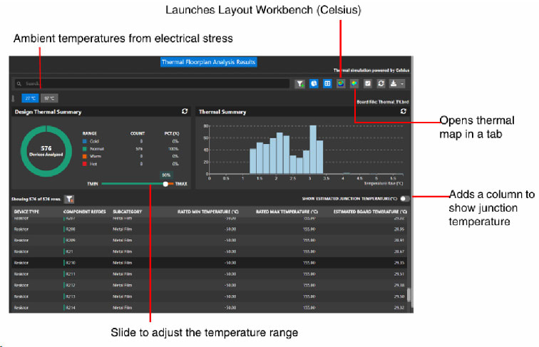
Thermal Floorplan Analysis Results dashboard integrated with Allegro X and Cadence Celsius Thermal Solver.
How Allegro X Helps in PCB Design for Space Applications
|
Feature |
Explanation |
How it Aids in PCB Design for Space Application |
|
High Voltage Constraint (HVC) Setup and Checks |
Ensures reliability by adhering to high voltage constraints, preventing electric discharge damage and potential fire hazards. |
Allows creation and assignment of high-voltage constraints, ensuring creepage and clearance distances are maintained. |
|
Import/Export High Voltage Constraints |
Facilitates adherence to design constraints and standards, ensuring high voltage handling capabilities are met. |
Enables importing and exporting constraints with high voltage settings for consistent design rules across different projects. |
|
Constraint-Driven Flow for High-Speed Interfaces |
Maintains signal integrity to prevent data corruption, optimizing data transmission performance in harsh space environments. |
Provides tools for setting up and verifying high-speed constraints, including differential pair routing and impedance control. |
|
Differential Pair Routing and Impedance Control |
Ensures reliable high-speed signal transmission and integrity, critical for data processing in space probes and rovers. |
Supports routing differential pairs and controlling impedance to meet high-speed design requirements. |
|
Pre- and Post-Layout Signal Integrity Analysis |
Identifies and resolves potential signal integrity issues before finalizing the PCB design, preventing data corruption. |
Offers signal integrity analysis tools to check and verify the performance of high-speed nets during both pre- and post-layout stages. |
|
AWR MWO-Allegro RF Design Flow |
Enhances RF signal transmission and reception, minimizing EMI/RFI interference for reliable RF communications in satellites. |
Integrates AWR Microwave Office (MWO) for importing RF blocks, facilitating RF design without grid conflicts. |
|
Generative AI for Optimal Design Solutions |
Accelerates the design process with intelligent design assistance, finding optimal solutions for complex PCB layouts. |
Uses AI to analyze design data, providing improved productivity, quality results, and efficient design closure. |
|
Hierarchical Design and Library Management |
Simplifies management of complex designs, ensuring consistency and reusability in PCB projects. |
Supports hierarchical schematic design and efficient library management, reducing design complexity and errors. |
|
Thermal Map Generation and Analysis with Celsius |
Enhances thermal management and heat dissipation, ensuring PCB performance and longevity under fluctuating space temperatures. |
Integrates with Celsius Thermal Solver to generate and analyze thermal maps, providing insights into thermal performance and hotspots. |
|
Metal Core PCBs |
Efficiently dissipates heat, essential in space environments to maintain electronic component performance. |
Supports the use of metal core materials (e.g., aluminum or copper) for better thermal management in PCB designs. |
|
MTBF Analysis Supporting FIDES Standard |
Identifies and prevents component failures early on, ensuring robust and reliable circuits for space missions. |
Provides Mean Time Between Failures (MTBF) analysis adhering to the FIDES standard, improving reliability predictions and assessments. |
|
Integrated Reliability Analysis and Stress Testing |
Produces robust circuits that can withstand harsh space environments by identifying overstressed components and design violations early. |
Offers tools for simulating and analyzing electrical stress, identifying and addressing overly stressed components without using SPICE or proprietary models. |
|
EMI Shielding Techniques and Filtering Components |
Reduces EMI/RFI interference, enhancing overall PCB design integrity and performance in space applications. |
Implements EMI shielding and filtering (e.g., ferrite beads, EMI filters) to mitigate electromagnetic interference. |
|
Differential Pair Routing and Ground Planes for EMI Reduction |
Ensures reliable electronic system operation by minimizing electromagnetic interference. |
Supports differential pair routing and the use of ground planes to reduce EMI, ensuring clean signal transmission and reception. |
Cadence Allegro PCB Design tools offer comprehensive solutions to meet the stringent requirements of PCBs for space applications. With features for high-speed, RF, and high-voltage design, Allegro ensures signal integrity and EMI protection, essential for space-grade PCBs.
Designers can leverage Allegro's advanced simulation and analysis capabilities to optimize thermal management and minimize outgassing, critical for long-term mission success. For more information, explore Cadence’s PCB Design and Analysis Software page to enhance your design process for space applications.
Leading electronics providers rely on Cadence products to optimize power, space, and energy needs for a wide variety of market applications. To learn more about our innovative solutions, talk to our team of experts or subscribe to our YouTube channel.