Component Placement Strategies in Multi-board PCB Systems
There are definitely limits on how much circuitry can fit on a single board. The board itself has an upper limit around the size of an extra-large pizza box for the sake of the fabrication equipment and standard panel sizes. The number of transistors on a device continues to balloon while the resistors and capacitors all but disappear to the unaided eye. Even with all of that integration and miniaturization, circuit complexity can grow to an unmanageable scale. One pizza isn't going to get the job done.
Expansion beyond the single PCB takes numerous forms. Telecom and other networking equipment often wind up in rack systems. The familiar 19 inch wide by 1.75 inch high rack unit is the default enclosure size for smaller circuits. This is what you picture when you read the words server farm or data center. From there, the baseline expands to multiple rack-units. Although they come in all sizes, a popular one is a seven rack-unit shelf; still 19 inches wide but it takes just over a foot of rack space. The shelf is populated with PCBs loaded in the vertical orientation, and they are connected using a 19" x 12" backplane that is assembled at the rear of the shelf.
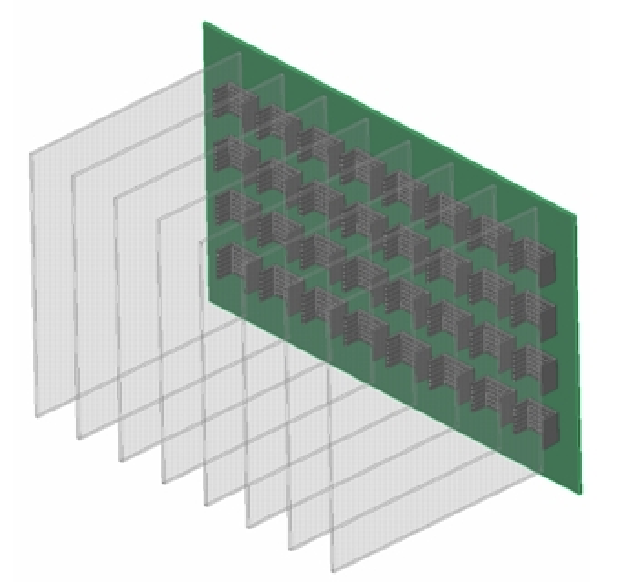
Image credit: Citeseer - The boards are only transparent for illustration purposes
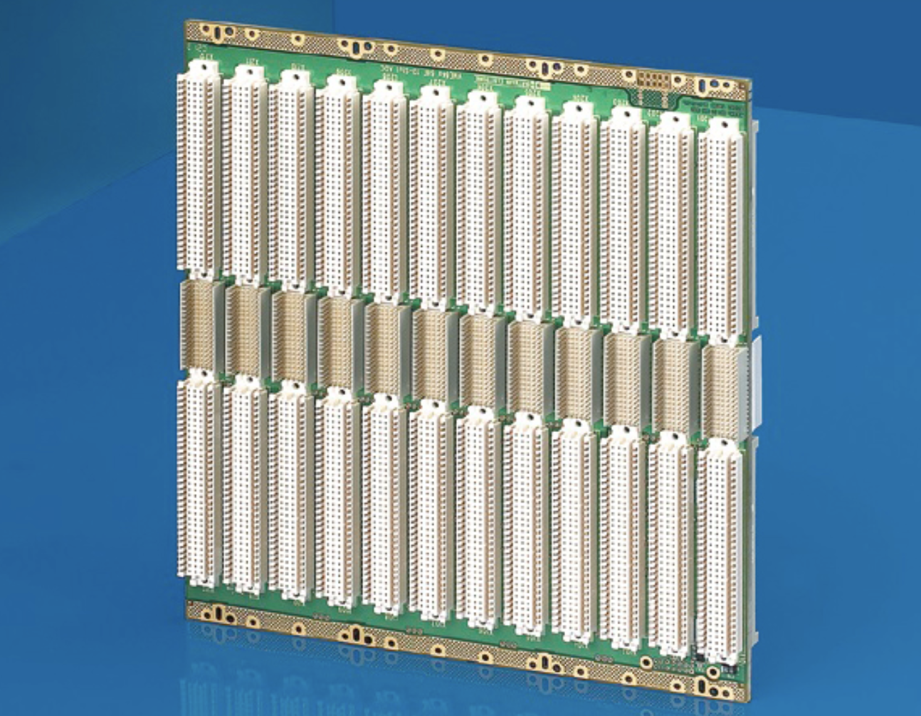
The backplane is typically nothing but connectors and routing. The layer count can be very high to support the mass of connectivity. The thickness of such a board provides the stiffness required to engage a 640 pin connector while working against anyone trying to preheat the backplane before soldering. For this reason, press-fit connectors are standard on these types of printed circuit boards.
Dealing With Thick PCBs
We often want some kind of housekeeping circuit in addition to the connectors. Those components will want to be surface mount, especially when the backplane is on the thicker side. Standard pins on through-hole parts do not have the length needed to reach the far side of the backplane so they would not be as solderable or rework-able. Then there are those previously mentioned pounds of copper used for ground planes to bring up to reflow temperature. Not pretty.
Another consideration related to board thickness is via stubs in the Z-axis. If you want to route from the top to layer 4 of a 24 layer board, those 20 other layers form a dangling line of sorts. If we go back in after all of the plating is done and drill a new, slightly larger hole right where the 20 layer stub was, we eliminate that discontinuity. Back drilling takes extra effort, but the results on the signal integrity eye diagram are measurable.
That brings us around to all of the other PCBs in the system. In a data center, you can expect some uniformity as the server blades fill most of the slots. The system is scalable with each new board adding to the overall performance.
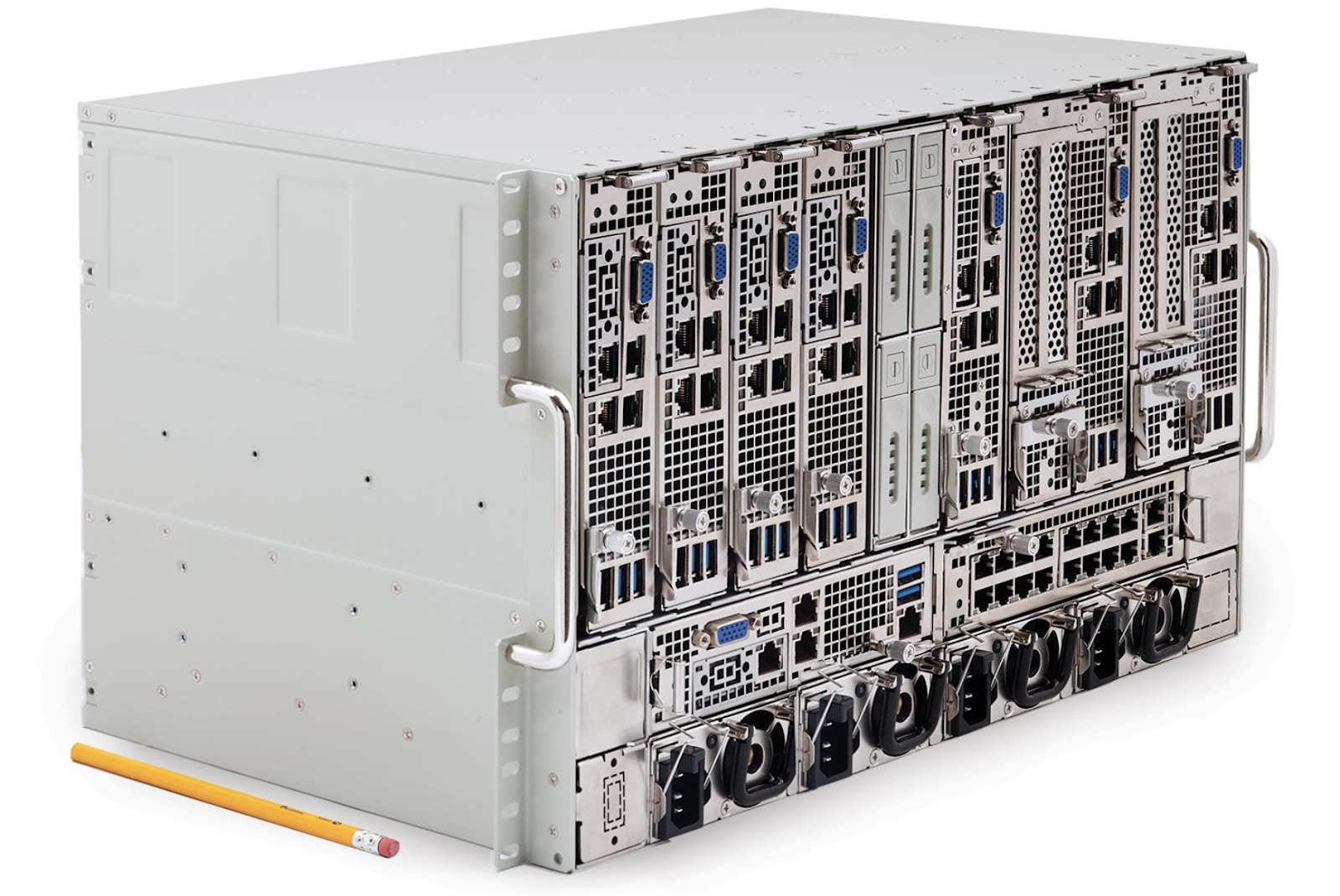
Photo credit: Mercury Systems- a mix and match approach to the system.
Other networking equipment can be more diverse. Each card slot is for a different purpose, and every card slot has to be populated for the entire group to work. The power supply is typically a stand-alone board because of all of the huge parts and extreme voltage swings that go along. The most current-hungry cards find a spot next to the power supply while the most sensitive victims hide in their own little box away from the heat and noise. Think of all of the gadgets that run off of a wall wart. The power supply is banished to the electrical socket and feeds the juice through a ferrite bead and/or a shielded cord to the rest of the system. Same principle.
The Good Neighbor Policy
Subdividing the rest of the schematic sections into boards is generally based on the block diagram. Just how those blocks are incorporated should be a function of the technology involved. Some circuits will demand high layer counts or aggressive HDI techniques. Others can live with a vanilla flavored four-layer board. Fine tuning around functionality and technology gets down to power domains, coexistence, thermal paths, weight distribution and finally aesthetics. I recall one board in a system being called the “tROtS board.” which stood for “the Rest Of the Story”. Sometimes, another word would replace “story”.
Not all systems require a seven foot high rack full of electronics to qualify. A few PCIe or SATA connectors may be all it takes. The example that comes to mind is a prototype version of Google’s “Home” mesh router. It was a larger form factor using yet another Qualcomm chipset. Three extra PCIe card slots gave it the capability to test the functionality of multiple router configurations. The air interface was another event. The only real way to test the wireless portion of the link is to build out a test-house. We enabled baseband level testing using a four-board system in the lab. The prototype was one of those cool 20% time things you used to hear about.

Image credit: Google
These mini systems may give you a little more latitude in terms of what goes where. Generally, the backplane is more of a motherboard that carries some of the computational load. In this case, your usual suspects need to be present on the big board. Memory and various drivers may find a home next to a microprocessor. Memory, of course, often lives on a SIM module that boils down to a board with a connector and a row of memory chips. In that respect, it can be considered another board for the system. Any lights, buttons, displays or other controls that are used once in the product end up on this layout. Then the plug-ins act as expansion slots when we want to add more capabilities. That was the model we used for the Google Home test vehicle.
A healthy multi-board system of this type will rely on some level of standardization. The daughter cards, in particular, will want to adhere to a protocol and may even be an off-the-shelf sub-assembly. In this case, the content of the line card (or whatever) is preordained.
As the world evolves towards the mesh network of 5G, the sub-systems will have to have replaceable and upgradable equipment at the cellular level and some serious bandwidth at the substation. The radios will have to be inexpensive, robust and ubiquitous. The centralized blocks will require unbridled throughput to go along with bulletproof reliability. The aggregating of all that data will not happen on a single board. Big networking is coming. Get ready.