Home
Free Trial
Home
Free Trial
Read More
Content
Filter
10 results found
Featured
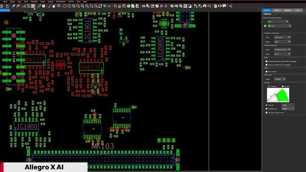
Danfoss Uses Cadence Allegro X AI to Amplify PCB Design for Energy Efficiency
Featured
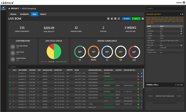
How to Optimize the Electronic New Part Introduction Process for PCB Design
Featured
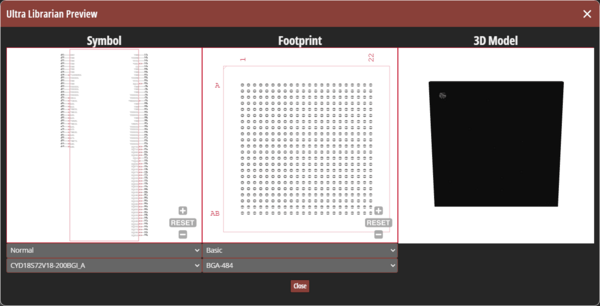
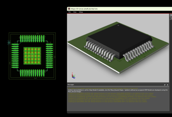
How to Use Verified Symbols, Footprints, and 3D Models for New Components in OrCAD X CIP
Featured
EMI Reduction Techniques for Switching Power Supply PCB Layouts
Featured
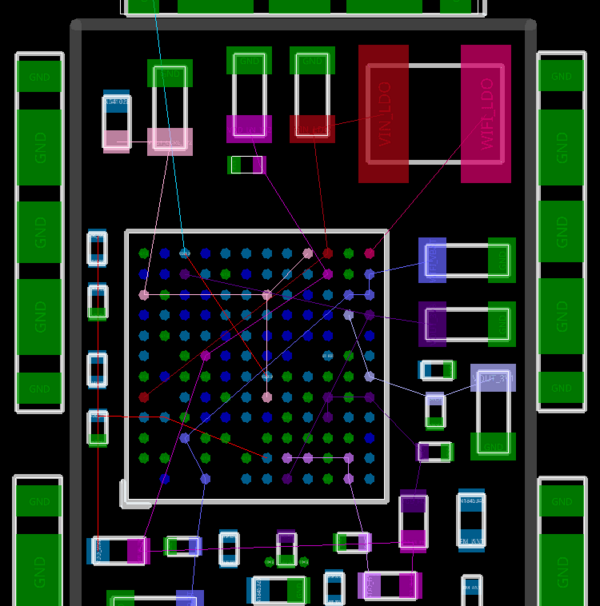
PCB Fanout For 0.4MM PITCH BGA Packages
Featured
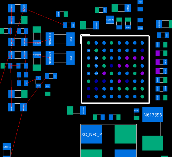
PCB Fanout For 0.5MM PITCH BGA Packages
Featured
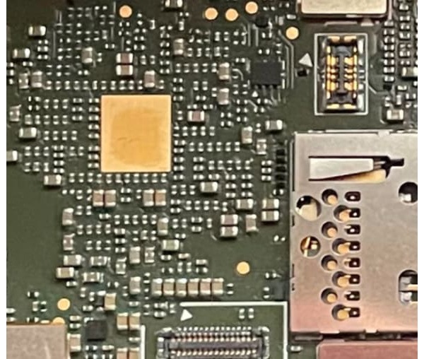
PCB Fanout For High Pin-Count BGA Packages
Featured
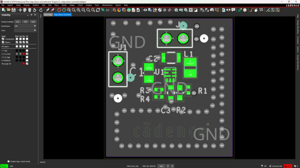
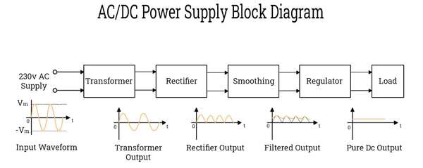
Alternating Current to Direct Current Converter Operation
Featured
Why PCB Data Management Is an Engineering Problem
Featured
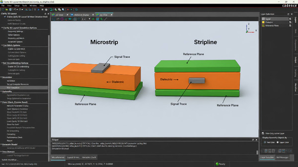
PCB Layer Stackup Design Strategies for EMI and Signal Integrity
Featured
Products
None
Allegro X PCB
(4)
Solutions
None
PCB Layout
(3)