High-Speed Signal Return Path Routing in OrCAD X
Key Takeaways
-
High-speed return currents follow the lowest impedance path, typically underneath the signal trace on the reference plane.
-
Poor return path design increases EMI, noise, and signal integrity issues.
-
OrCAD X helps define constraints and layers for return path with automatic Design Rule Check, ensuring a stable PCB design.

A return path in PCB design is the route that electrical current follows back to its source after traversing through a load, traces, or circuit components. Although a return path may seem evident in schematic diagrams, it becomes less intuitive in PCB layouts due to the complexity and three-dimensional nature of the physical layout. Effective management of high-speed signal return paths will minimize electromagnetic interference (EMI), impedance discontinuities, and signal integrity issues.
High-Speed Signal Return Path Management
The return path in a PCB is influenced by the frequency of the signal. While DC signals follow the path with the least resistance, high-frequency signals seek the path of least impedance, typically directly beneath the signal trace in the reference plane. Mixed-frequency signals introduce additional complexity, requiring careful PCB layout to prevent unwanted interference. A properly designed return path enhances electromagnetic compatibility (EMC), reduces noise, and prevents potential signal integrity degradation by providing a low-impedance, continuous pathway.
High-Speed Signal Return Path Tips
|
Return Path Tips |
Purpose |
|
Use Solid Ground Planes |
Ensures low-impedance, continuous return paths for stable signal integrity. |
|
Avoid Gaps and Splits |
Prevents disruptions in the return path. Cutouts, slots, or clearances in the ground plane increase loop inductance and EMI. |
|
Maintain Short and Direct Paths |
Minimizes impedance, and enhances electromagnetic compatibility (EMC). |
|
Manage Mixed-Signal Designs |
Prevents digital signals from interfering with analog circuits. Ensure proper signal-layer-to-ground-layer alignment for controlled impedance and reduced noise. |
Setting Up Return Path Constraints in OrCAD X
OrCAD X Constraint Manager can help you define constraints for high-speed signal return paths. Follow these steps to set up return path constraints in OrCAD X.
Step 1: Open the Constraint Manager
-
Navigate to Constraint Manager in OrCAD X.
-
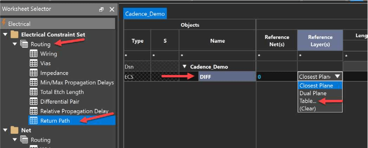
Open the Electrical Workbook and go to Routing > Return Path.
Step 2: Create an Electrical Constraint Set (ECSet)
-
Right-click on the DSN cell name
-
Select Create Electrical CSet, enter a name, and add it to the ECSet list.
-
If a change is needed, update the rule definition, and all assignments will automatically update.

Step 3: Assign Reference Net and Layer
-
Set the Reference Net (typically GND (0)) to define the return path.
-
Define the Reference Layer(s) based on signal routing behavior:
-
Closest Plane: automatically selects the nearest ground/power plane.
-
Dual Plane: ensures reference above and below signal layers.
-
Table Option: explicitly define return path layers for each signal layer.

Step 4: Configure Return Path Constraints
Define key constraints to manage return paths effectively:
|
Constraint |
Purpose |
|
Max Pad Gap |
Defines the maximum gap allowed in the return path for pad escapes (e.g., through-hole connectors). Checked when the entire trace width enters a Pin and Via void in the reference plane. |
|
Length Ignore |
Specifies how far a signal can travel without a return path before a Design Rule Check (DRC) violation occurs. Checked when the trace centerline crosses an opening in the reference plane. |
|
Stitching Via Distance |
Ensures that a stitching via is placed within a specified distance of a signal via transition, maintaining a continuous return path. Defines a square search area for signal via transitions. |
|
Adjacent Void Spacing |
Prevents return paths from running too close to plane edges or voids (e.g., Pin/Via voids), reducing EMI risk. Supersedes any Length Ignore/Pad Gap rules to account for fabrication shifts. |

Closest Plane and Max Pad Gap rules applied in OrCAD X
Step 5: Apply Constraints to Nets
-
Open the Net Workbook in the Constraint Manager.
-
Assign the return path ECSet to the required nets.
-
The system automatically checks for Design Rule Check (DRC) violations, such as:
-
Void crossings
-
Excessive pad gaps
-
Missing stitching vias
-
- Cross-probe errors to locate and fix design violations.
Step 6: Verify and Monitor Return Path Violations
-
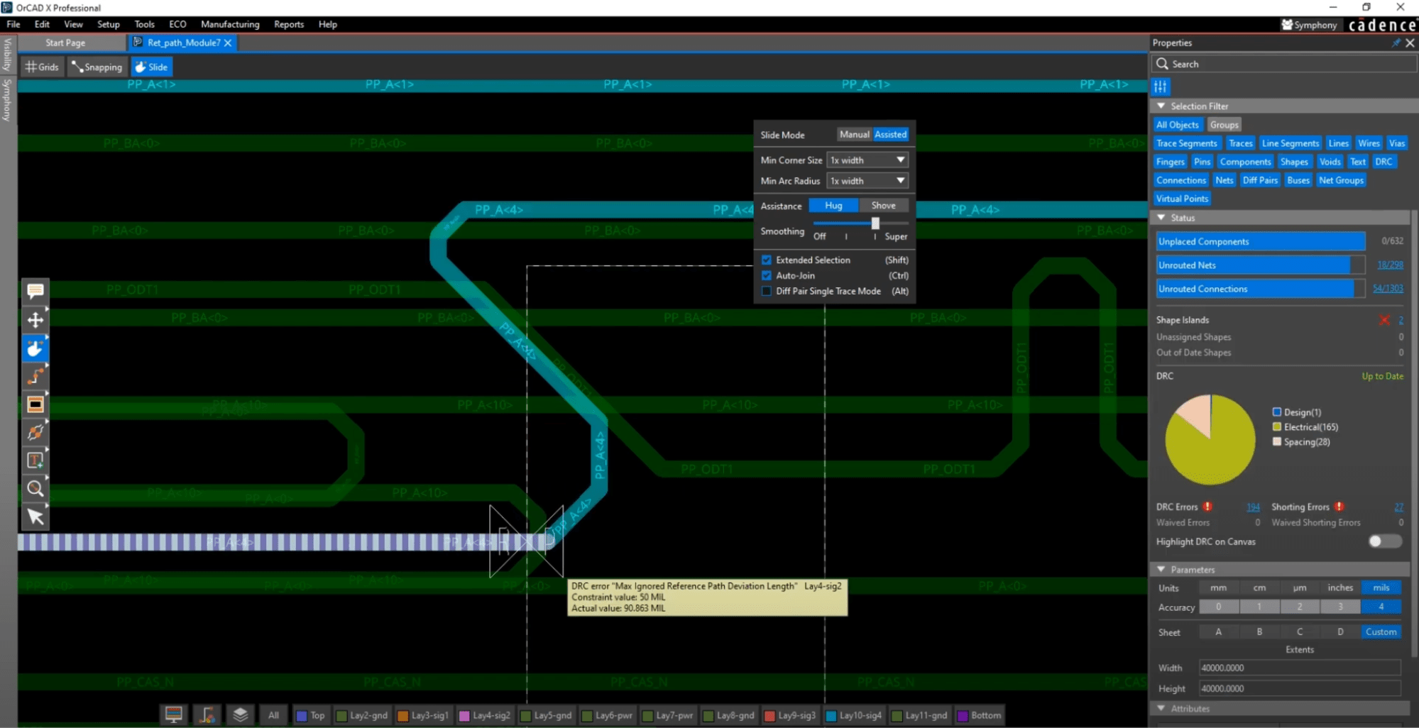
Real-time DRC checks can identify and fix return path violations instantly.
-
If a violation occurs (e.g., missing ground continuity), cross-probe to locate and resolve the issue.
-
Turn on the ground layer view to verify that the return path is continuous.
-
Fix violations such as cutouts in the ground plane to restore proper return paths.

Proper management of high-speed signal return paths is essential for reducing EMI and maintaining signal integrity in PCB designs. OrCAD X provides powerful tools to define return path constraints, set reference layers, and enforce design rules, ensuring optimal performance. explore OrCAD X for robust return path management.
Leading electronics providers rely on Cadence products to optimize power, space, and energy needs for a wide variety of market applications. To learn more about our innovative solutions, subscribe to our newsletter or our YouTube channel.