PCB Fault-Finding Techniques With OrCAD X
Key Takeaways
-
PCB fault-finding focuses on the cause of defects; while it technically falls under the manufacturers’ domain, designers can also limit defects to improve the manufacturers’ failure analysis.
-
Constraint-driven design will always limit design mistakes and manufacturing defects.
-
OrCAD X can rapidly examine DRC violations with the DRC Browser and ensure manufacturing output is always up-to-date with Live DOC.
PCB fault-finding techniques start with thoroughly covering design rules with the Constraint Manager.
PCB design and manufacturing is an iterative process: only a certain amount of design and simulation performance can be accounted for before the rubber meets the proverbial road. Sometimes, manufacturing solutions are straightforward: supply chain cost/availability of certain materials or sub-products may necessitate a design revision. Other times, like when performing fault analysis, the path forward becomes less clear.
While fault analysis typically falls under the purview of the manufacturer, the designer can aid the process with PCB fault-finding techniques to ensure their design meets all manufacturing requirements and stipulations according to industry standards. From the design end, PCB fault-finding techniques focus on crafting constraint rules that accurately reflect the manufacturing equipment's precision and tolerance.
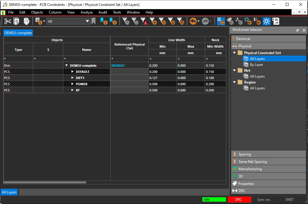
Constraint Manager Design Rules by Type
|
Electrical |
General routing and net-specific rules for topology, stub length, via structure, target impedances, propagation delays, differential pair characteristics, and return pathing. |
|
Physical |
General, net-specific, and region-defined rules for line width, spacing, differential pair characteristics, via structure, and microvia stagger. |
|
Spacing |
Spacing rules for different-net board objects. |
|
Same Net Spacing |
Spacing rules for same-net board objects. |
|
Manufacturing |
Fabrication, assembly, and testing rules for copper features/solder masking (openings, pads, annular rings, etc.), silkscreen, paste mask, and test points. |
|
3D |
Spacing rules for 3D bodies (component-component, component-board edge) and rigid-flex. |
|
Properties |
Miscellaneous net properties like frequency, period, duty cycle, backdrilled, shielded, etc. |
Setting Up a Constraint-Driven Design: A Key PCB Fault-Finding Technique
Setting up design constraints acts as a guardrail for the designer by providing live reporting when a design no longer observes the pre-defined constraints. Design constraints can and do evolve throughout a design, but unlike the layout, design constraints should be settled early by discussing internally with engineering or consulting the manufacturer. Only in the face of a change to design or manufacturing scope should users alter the general design rules (specific instances of design rule applications, i.e., extra spacing around a particularly noisy trace, would be an exception to this rule of thumb). Keeping the design rules more or less constant avoids expanding design rework unnecessarily and limits the chance of “obscured” errors or incorrect designs sent to the manufacturer.
A designer should never send manufacturing files out while a DRC still throws errors – this should be one of the last checks (and even double-checks) before finalizing documentation. However, when DRC flags are still present in a design (for example, a new revision with significant changes to the Constraint Manager ruleset), users can look through a sortable list of DRC errors in the DRC Browser.
Launched from the Constraint Manager, the DRC Browser has an easily navigable list of all design rule violations in the design and synchronizes to the layout, giving designers an easy way to track and correct violations. The left column of the DRC Browser has a collapsible list where users can expand DRC flags by type of violation. The right column contains a breakdown of the violation, including location, conflicting object(s), and constraint source. By right-clicking an entry in the right column, users can jump to the flag in the layout, mark it for review, or waive the violation.
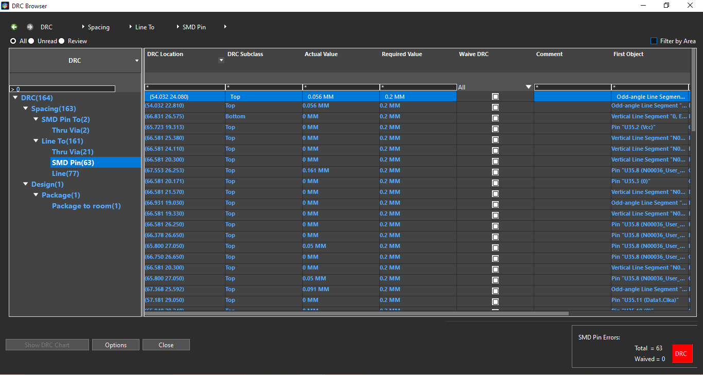
Users can scroll through all of the board violations in the DRC Browser.
The DRC Browser can also output the list of DRC violations as a more readable bar or pie graph. Users can further specify a breakdown by DRC violation type.
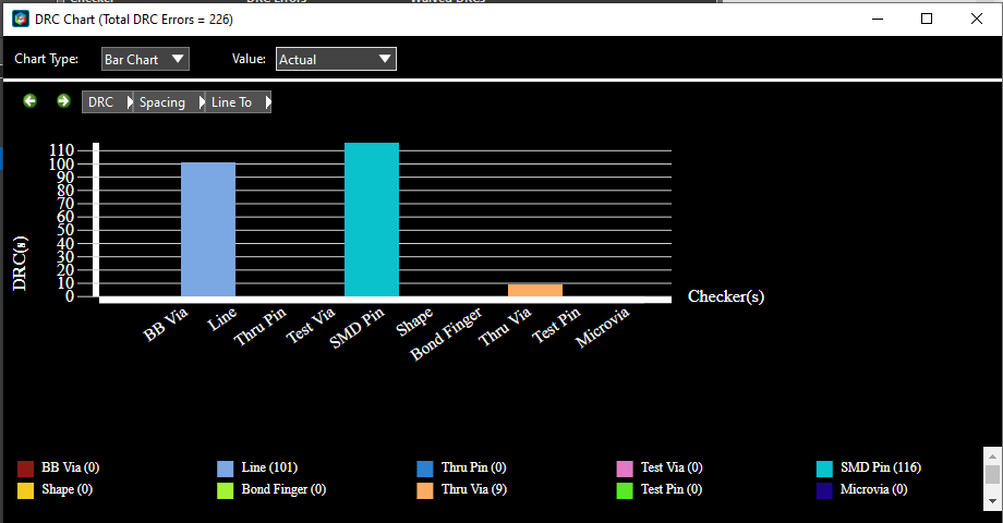
It’s also possible to show DRC Browser results as a graph.
More PCB Fault-Finding Techniques for Designers
Designers can use OrCAD X Presto PCB Editor reporting to see a searchable and sortable list of various potential layout and manufacturing issues, including:
- Shape islands
- Unassigned shapes
- Missing teardrops
- Missing tapers
- Dangling vias, traces, and antenna
When designing PCB layouts, it’s critical to be proactive and prevent defects before they occur during manufacturing or in service life.
-
Carefully review design rules; a manufacturing or runtime issue may be unflagged if it falls outside the ruleset (for example, same-net spacing rules versus global net spacing rules).
-
Talk with the manufacturer to ensure the design and manufacturing goals align. While it’s the manufacturer's job to meet the design's framework, stackup, placement, or routing decisions may be unnecessarily demanding. When appropriate, relax design constraints to maximize yield and minimize defects.
-
Review supplier/vendor data and component manufacturers’ datasheets to ensure a fit between design intent and material properties.
PCB Fault-Prevention Techniques: OrCAD X Live DOC Environment
The best PCB fault-prevention technique is to carefully manage manufacturing documentation to ensure the design conveyed through various output files is representative of the layout’s design intent.
One of the best tools for designers in OrCAD X Presto PCB Editor is the Live DOC environment, which synchronizes all manufacturing outputs to the layout. Any updates to the layout show up instantaneously in the Live DOC templates, ensuring that documentation and design updates always correspond. Live DOC also makes it easy to switch between manufacturing documentation with predefined and user-customizable templates that capture all the necessary layout information for a seamless transition to PCB production.
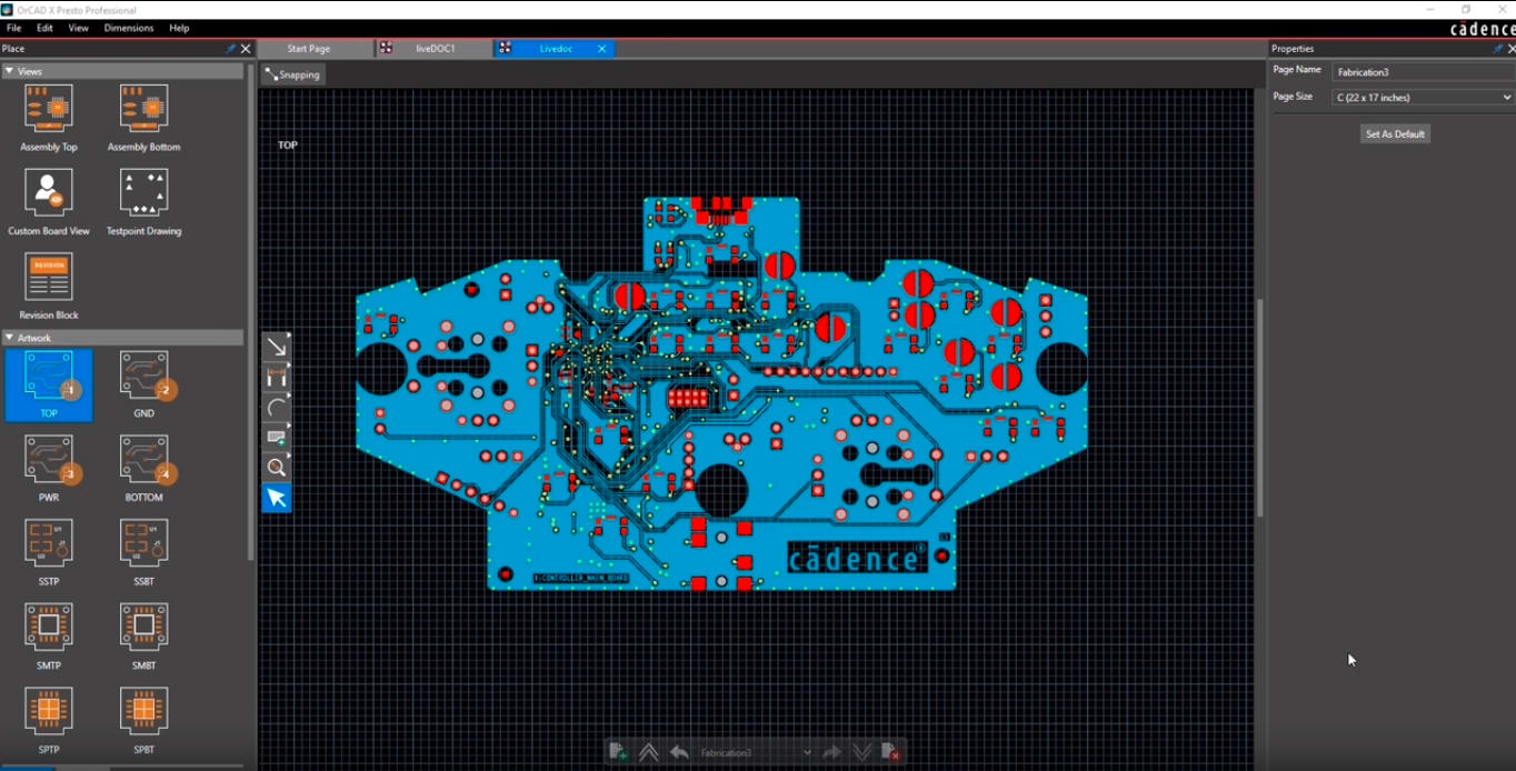
Live DOC ensures documentation is always up-to-date with the board design.
The Best PCB-Fault Finding Technique? Use OrCAD X
PCB fault-finding techniques on the design end focus on a proactive approach to preventing manufacturing defects, unlike the reactive fault analysis that manufacturers employ through destructive and non-destructive testing. By carefully crafting the design rules to fully encapsulate all of the PCB’s manufacturing and performance requirements, designers can greatly limit the occurrence and severity of manufacturing defects.
With the new OrCAD X platform, it’s easier to ensure a seamless transfer of design intent from layout to manufacturer with the new Live DOC feature. Interested in further improving manufacturing outcomes? See how Cadence PCB Design and Analysis Software prepares designs for manufacturing while optimizing cutting-edge performance.
Leading electronics providers rely on Cadence products to optimize power, space, and energy needs for a wide variety of market applications. To learn more about our innovative solutions, talk to our team of experts or subscribe to our YouTube channel.