Managing Constraints in OrCAD X
Key Takeaways
-
OrCAD X provides structured workflows, net grouping, and reusable constraints to save time and reduce errors.
-
Use constraint regions for precision in dense or high-speed areas, ensuring compliance with design requirements.
-
Features like cross-probing link schematics and layouts, and streamlining design verification.
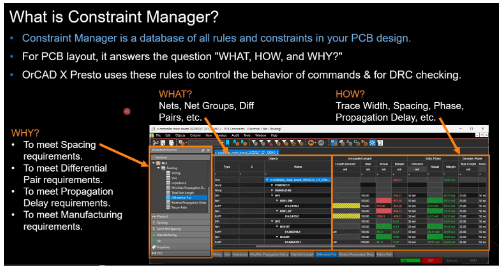
Basics explaining what is a constraint manager in OrCAD X.
Managing constraints in OrCAD X is critical for creating efficient, reliable, and manufacturable printed circuit board (PCB) designs. Constraints ensure that a PCB meets operational, manufacturing, and functional requirements. This guide summarizes key takeaways and processes from a webinar on constraint management in OrCAD X, providing a detailed overview of tools, methodologies, and best practices.
PCB Design Constraints in OrCAD X
PCB design constraints are sets of rules that ensure your circuit works as intended and can be manufactured efficiently. These constraints address various aspects of the design, such as mechanical, thermal, electromagnetic, and manufacturing requirements. However, PCB constraints are unique compared to general engineering rules because they integrate inputs from multiple parts of your board and manufacturing requirements.
-
Multidisciplinary Nature: PCB constraints are influenced by electrical engineers, mechanical engineers, manufacturers, and even component suppliers. For example, an electrical engineer might specify signal integrity requirements, while the manufacturer determines the minimum trace width for fabrication.
-
Layer-Dependent Rules: Unlike single-domain engineering, PCB design involves multiple layers (both physical and electrical), making constraint management a multi-dimensional problem.
-
Dynamic Adjustments: Constraints must be flexible enough to adapt during the design process as simulation results or manufacturing feedback require changes.
-
Tool Integration: Modern PCB design tools like OrCAD X streamline constraint management by allowing rules to flow seamlessly between schematics and layout, minimizing errors and improving consistency.
How to Make Effective PCB Constraints
|
Category |
Description |
Examples and Details |
|
Structured |
Organize constraints systematically to avoid confusion. |
- Use net groups or buses to categorize signals (e.g., power nets separate from signal nets). |
|
Verifiable |
Every constraint should be testable using design tools. |
- Use tools like OrCAD X Design Rule Checks (DRC) or Constraint Manager. |
|
Repeatable |
Constraints should be reusable across designs for efficiency. |
- Enable re-creation of designs without re-entering rules if netlist and components remain unchanged. |
|
Specific |
Constraints should address particular design scenarios to meet requirements. |
- Define gap and impedance for differential pairs to meet high-speed requirements. |
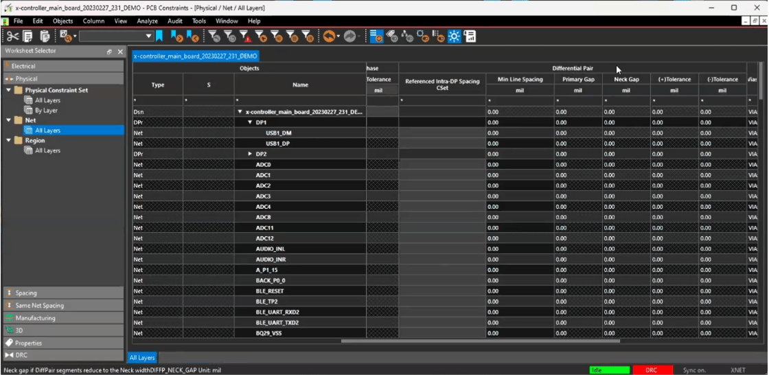
Setting constraints for a differential pair includes electrical constraints, physical constraints, and spacings.
Managing Constraints in OrCAD X With The Constraint Manager
Managing constraints in OrCAD X is not just about creating rules, but organizing, applying, and refining them to ensure a seamless and manufacturable design process. Below, we’ll dive into each step with detailed strategies and practical tips.
Setting Up Default Rules for Manufacturability
Default rules serve as a baseline for your design, ensuring that even if no specific constraints are applied, your PCB will meet fabrication standards. Default rules are important because of the following:
-
Manufacturers have minimum capabilities, such as trace width, spacing, and via dimensions, that must be adhered to.
-
Default rules act as a fallback for nets that don’t have specific constraints assigned.
Where to Define Default Rules in OrCAD X
-
In OrCAD X Constraint Manager, navigate to the Physical Worksheet under All Layers to set up global rules for trace width, spacing, and neck width.
Grouping Similar Signals for Efficient Management
Net grouping is a powerful way to streamline constraint applications and maintain organization in complex designs.
How to Group Nets:
-
Use OrCAD X Constraint Manager to create net groups or net classes. Group all power nets, signal nets, or high-speed nets into categories for easier rule application.
Benefits of Grouping Nets:
-
Reduces repetitive work—apply one constraint set to an entire group.
-
Simplifies error tracking—violations are easier to pinpoint within a group.
Best Practices:
-
Name groups descriptively, such as "Power_Nets_5V" or "HighSpeed_USB", to easily identify their purpose.
-
Include all differential pairs in a separate group for specialized constraints.
Creating and Naming Constraint Sets
Constraint sets define the actual rules applied to net groups and should be tailored to the specific needs of your design.
What Are Constraint Sets:
-
They specify physical and electrical characteristics such as trace width, spacing, and impedance for groups of nets or individual nets.
How to Create Constraint Sets:
-
In Constraint Manager, right-click in the Physical Constraint Set section and create a new set. Assign trace width, neck width, spacing, and any special requirements like via types or maximum etch lengths.
Why Descriptive Names Matter:
-
Use names like "Signal_10mil", "Power_20mil", or "Critical_HighSpeed". These names ensure clarity, especially in multi-designer teams or when reusing constraints in future projects.
Avoiding Individual Rule Overrides
Maintaining organized and consistent constraints is key to effective PCB design.
-
Risks of Individual Rule Overrides: Overriding individual rules creates a scattered and disorganized constraint structure. This makes debugging errors difficult because overrides may not be reflected in global rules.
-
Best Practice: Always update the constraint set rather than individual rules. This ensures that all nets within a group adhere to consistent standards.
Real-World Application: OrCAD X Presto Demo Highlights
Assigning voltages to power nets allows for better visualization and simplifies routing.
Assigning Voltages to Power Nets
Setting voltages cleaned up routing visuals by replacing the “rats nest” of connections with simple indicators for internal planes.
-
Steps Taken:
-
Power nets like USB_5V and VDD_3.3V were assigned their respective voltages.
-
This eliminated unnecessary visual clutter and allowed for a better focus on signal traces.
-
Impact:
-
Enhanced clarity in routing visuals.
-
Simplified routing by automatically directing power nets to planes.
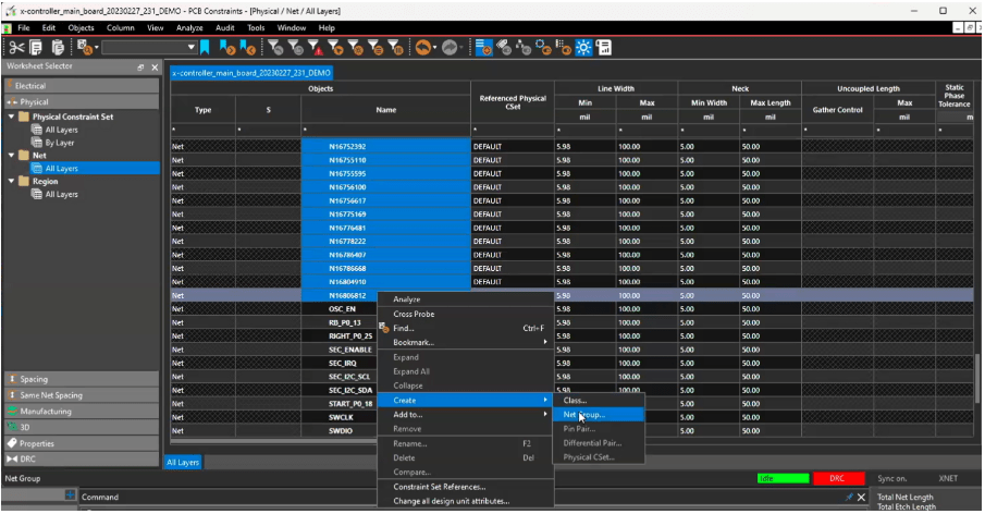
Creating net grouping in OrCAD X: select nets, right click > create > net group.
Creating and Applying Constraint Sets
The demo showcased how managing constraints in OrCAD X can be done with net groups that were created and assigned specific constraint sets. Custom constraint sets (e.g., for signal and power nets) were defined and applied to net groups, ensuring consistent design rules.
-
How It Was Done:
-
Signal nets, power nets, and critical nets were grouped into categories using Constraint Manager.
-
Custom constraint sets (e.g., Signal_10mil, Power_20mil) were applied to each group.
-
Key Benefits:
-
Consistency in rules across similar nets.
-
Simplified adjustments—modifying the constraint set automatically updated all associated nets.
Using Constraint Regions for Localized Rules
The demo highlighted the use of constraint regions for areas with unique routing requirements. A specific constraint region was created to handle narrower trace widths near a dense connector area, demonstrating the flexibility of regional constraints.
-
What Are Constraint Regions:
-
Specific areas on the PCB where constraints differ from the global rules.
-
Useful for dense layouts, high-speed components, or connector areas.
-
Demo Example:
-
A constraint region was created near a connector with narrower trace widths (7 mils instead of the default 10 mils) to accommodate tighter spacing.
-
The designer routed traces into the region, and OrCAD X Presto automatically adjusted the trace width.
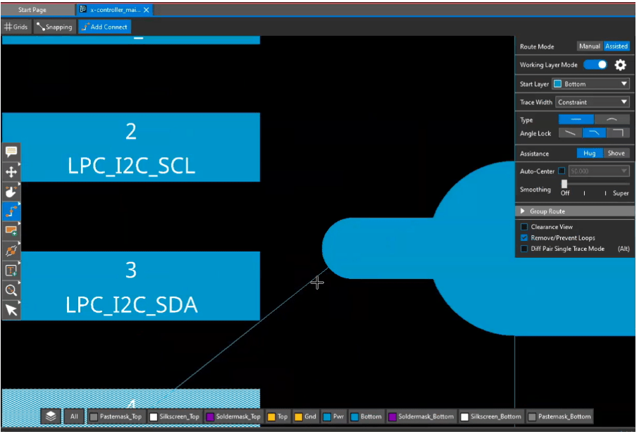
Routing in real-time the trace width automatically shrinks as it approaches the vicinity of the pads of an IC.
Cross-Probing Between Schematics and Layout
The demo emphasized the importance of cross-probing for verifying constraints.
-
How Cross-Probing Was Used:
-
The designer selected nets in the schematic, which highlighted them in Constraint Manager and the PCB layout.
-
This allowed the designer to verify which nets belonged to which net group and ensure proper constraints were applied.
-
Benefits:
-
Quick identification of design rule violations.
-
Improved collaboration between schematic and layout teams.
Reusing Constraint Sets Across Designs
The demo demonstrated how managing constraints in OrCAD X can be done using constraint sets that are exported and reused in future projects.
-
Steps Taken:
-
The designer exported a constraint set for high-speed differential pairs.
-
In a new project, this set was imported, saving time and ensuring consistent design rules.
-
Practical Applications:
-
Particularly useful for repetitive designs or standardized interfaces like USB, HDMI, or DDR memory.
Managing constraints in OrCAD X can be accomplished by following these practices. OrCAD X simplifies this process with advanced tools for net grouping, constraint regions, and cross-probing. Learn more about OrCAD X features and how it supports efficient PCB design by visiting Cadence’s PCB Design and Analysis Software page.
Leading electronics providers rely on Cadence products to optimize power, space, and energy needs for a wide variety of market applications. To learn more about our innovative solutions, talk to our team of experts or subscribe to our YouTube channel.