How to Improve PCB Design Workflow
Key Takeaways
-
Effective component, design and product lifecycle data management are key attributes for electronic product design, deployment and reliability.
-
Understanding the challenges is essential in determining how to improve PCB design data management.
-
OrCAD X has various capabilities that enable you to optimize your PCB design workflow.
There are a variety of numerous tips you can use to improve PCB design.
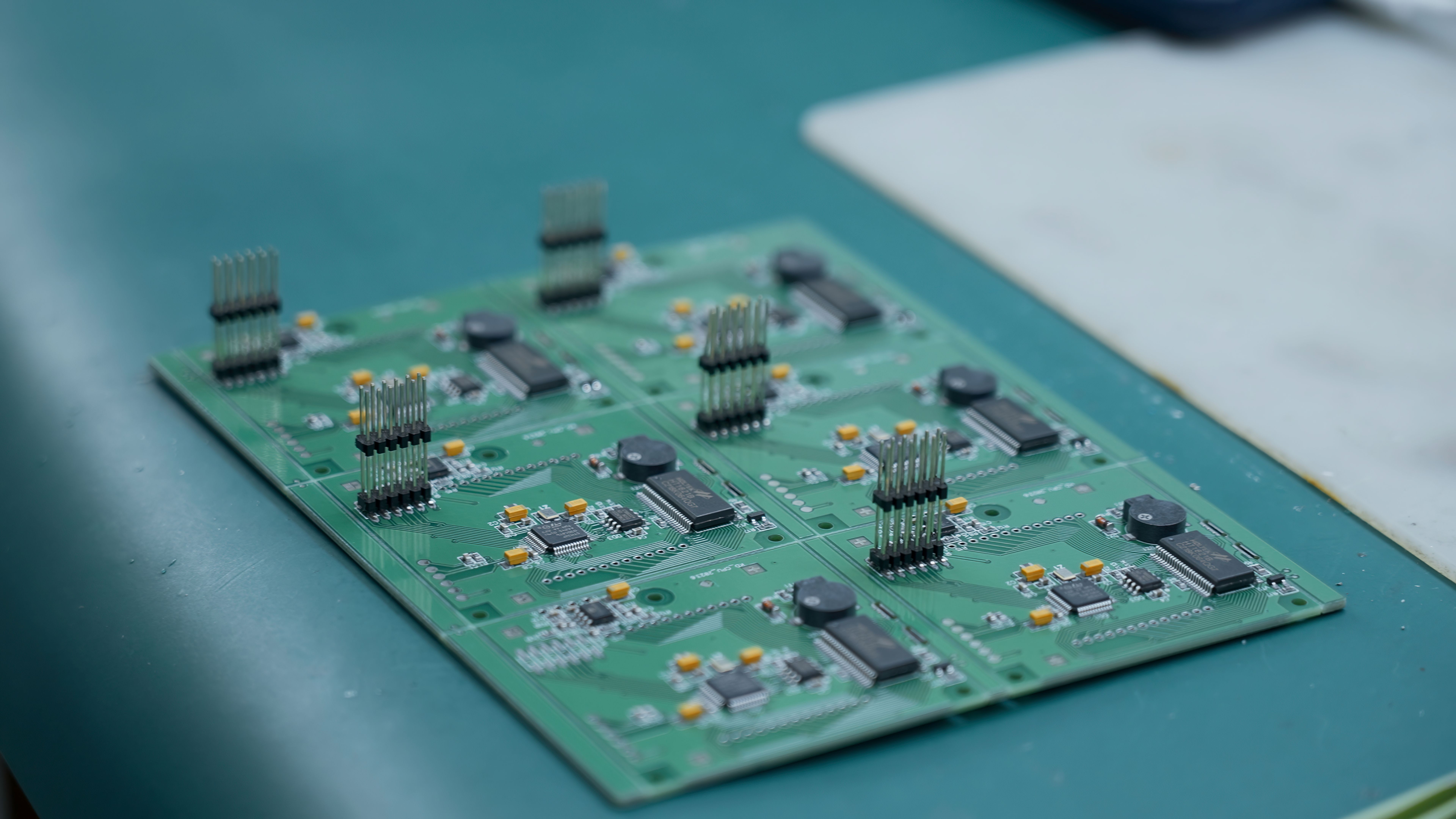
PCB design is an incredibly involved process with numerous details, from component selection to final layout. As engineers constantly push boundaries, the question of how to improve PCB design often comes up. Some aspects of improving PCB design include optimizing the physical layout and efficiently managing the data that flows throughout the design process. Read on as we discuss key strategies for improving PCB design, focusing on data management as a critical element.
How to Improve PCB Design With Optimized Data Management
For extremely large projects, effective data management is an important method of improving PCB design. With a lot of (usually metaphorically) moving parts and different integration needs, ensuring that processes are streamlined, errors are minimized, and collaboration is accessible is important.
|
Key Areas of Data Management |
|
|
Data Management Type |
Description |
|
Component Data Managemen |
Managing selection, verification, and sourcing of components, ensuring availability and compatibility. |
|
Organizing and controlling all design-related files, including schematics, layouts, and documentation. |
|
|
Integrating design data with manufacturing, supply chain, and end-of-life management. |
|
Efficient design data management can improve PCB design by organizing and controlling design files, such as schematics and layouts, to maintain consistency and prevent data loss. PLM integrates design data with manufacturing and supply chain processes, ensuring that product development aligns with market needs and lifecycle stages.
Advanced and involved PCB design faces challenges such as data silos, version control issues, and managing component availability. Breaking down these silos, implementing robust version control using advanced PCB software, and using real-time data management tools are essential steps to overcoming these obstacles. Additionally, integrating design data with manufacturing requirements through PLM can bridge gaps and improve the overall design process. Addressing these challenges is key to achieving high-quality, efficient PCB designs.
General Tips For Improving PCB Design
Important tips for improving PCB design regarding traces and copper include adequate spacing between traces to prevent short circuits, balancing copper distribution across layers to avoid warping, and using 45-degree trace angles to prevent etching issues.
-
Using as many solid copper layers for power planes aids in EMI shielding and heat sinking, and adding fiducials enhances surface mount assembly accuracy. For dense designs, buried vias can maximize routing space, and a symmetrical stack-up improves board stability.
-
For connecting your board to the broader device, mounting hole placement is crucial—ensuring they have sufficient clearance and are positioned thoughtfully to avoid interference with other components.
-
The silkscreen layer, often overlooked, is valuable "real estate" for documenting important information like labeling connectors and components.
Find a Mentor
Improving PCB design involves several factors, and one of the most effective ways is by working with a mentor. Many consider PCB design almost an art form, and there are many nuanced techniques that can be learned from someone who has mastered the craft. Presenting your design to an experienced individual can provide invaluable insights and help you refine your skills.
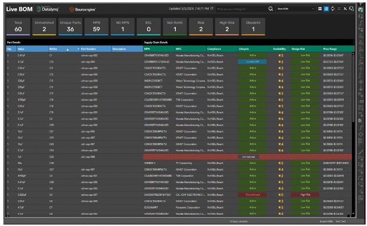
OrCAD X Live BOM shows details on component parts and the supply chain.
How to Improve PCB Design with OrCAD X
|
PCB Area |
OrCAD X Feature |
Description |
|
Design Rule Checks (DRC) |
DRC Manager |
Automatically checks for violations in the design, ensuring compliance with specified rules. |
|
Signal Integrity |
Topology Explorer |
Provides tools to analyze signals, reducing noise and ensuring proper signal performance. |
|
Power Integrity |
Power-aware Simulation |
Simulates power distribution networks to identify issues and optimize power delivery across the PCB. |
|
Impedance Controlled |
Controlled Impedance Design |
Helps design and verify controlled impedance traces critical for high-speed designs. |
|
3D Design and Visualization |
3DX Viewer |
Enables 3D visualization of the PCB layout to check for mechanical fit and clearance issues. |
|
Design for Manufacturability |
DFM Checker |
Ensures that the PCB design meets manufacturing constraints, reducing errors during production. |
|
Component Placement |
Auto-placement Tools |
Assists in the optimal placement of components based on design constraints and performance considerations. |
|
Routing Optimization |
Interactive router |
Improves routing efficiency, allowing for better signal integrity and shorter routing paths. |
|
Collaboration with Mechanical Design |
ECAD-MCAD Co-Design Tools |
Facilitates collaboration between electronic and mechanical design teams for integrated product development. |
|
Version Control |
Integrated Version Control |
Tracks design changes and allows for effective management of design iterations and team collaboration. |
|
Reliability Analysis |
Stress and Reliability Analysis |
Assesses the PCB design for long-term reliability under various stress conditions. |
|
Design Documentation |
Automated Documentation Generation |
Produces detailed and accurate documentation for manufacturing, assembly, and testing processes. |
OrCAD X for Data Management
OrCAD X integrates seamlessly with product lifecycle management (PLM) systems through OrCAD X Engineering Data Management (EDM), aligning design data with manufacturing and supply chain processes for a cohesive product development cycle. Additionally, its component data management features, facilitated by Live BOM, ensure efficient selection, verification, and sourcing of components, improving PCB design for large, involved projects.
Effective data management and integration with manufacturing processes are essential to understanding how to improve PCB design. The Cadence OrCAD X platform offers powerful tools to optimize your design workflow, from advanced component management to real-time collaboration features. To learn more about improving your PCB design, explore our PCB Design and Analysis Software and discover the innovative capabilities of the new OrCAD X platform.
Leading electronics providers rely on Cadence products to optimize power, space, and energy needs for a wide variety of market applications. To learn more about our innovative solutions, talk to our team of experts or subscribe to our YouTube channel.