Design for Manufacturing (DFM)
Key Takeaways
- DFM can be described as the combination of two methodologies: design for fabrication (DFF) and design for assembly (DFA).
- DFF and DFA ensure products are designed to be manufactured and assembled efficiently and easily.
- The three phases of the DFM process are the design phase, the component placement phase, and the routing phase.
DFM intends to challenge the design stage at all levels.
A PCB designer must consider the standards and limitations of the PCB manufacturer to ensure the design and manufacturing process goes smoothly. For this reason, PCB design for manufacturability (DFM) should adhere to all the requirements of board design. Read on as we discuss DFM best practices for printed circuit boards.
Design for Manufacturing (DFM)
DFM is closely related to design for fabrication (DFF) and design for assembly (DFA).
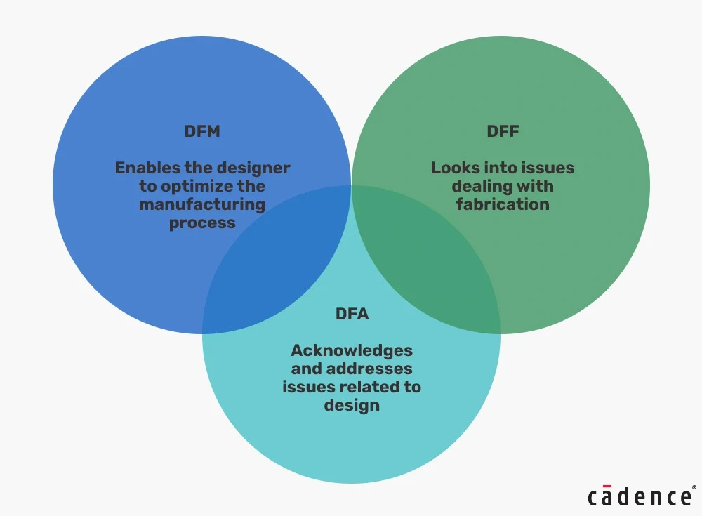
DFM, DFA, and DFF compared.
DFF and DFA ensure the product is designed for efficient manufacturing and assembly. DFM best practices are adhered to by product development companies to prevent, detect, quantify, and reduce inefficiencies and waste in the PCB manufacturing process.
PCB design for manufacturability (DFM) involves optimizing a PCB layout, ensuring a smooth fabrication and assembly process. All problems associated with PCB design can be mitigated through proper DFM processes.
When optimizing the product development process, one of the major areas to improve is the PCB layout design for manufacturing. If the PCB is designed with DFM principles in mind, it undergoes necessary design changes aimed at reducing manufacturing costs and ensuring compliance with manufacturing, fabrication, and assembly rules, thus streamlining the production process.
DFM intends to challenge the design stage at all levels. The DFM process checks the accuracy of the design at the system level, sub-system level, and component level. These all-level process checks ensure the design is optimized and cost-effective.
Advantages of Following DFM Practices
- Fewer Iterations: Regarding PCB manufacturing, money is often wasted on redesigns. DFM reduces the number of iterations and redesigns by taking into account all the limitations and challenges of the vendors and cost parameters from the start.
- Faster Time-To-Market: Assembly and installation take less time when DFM principles are followed. DFM reduces the need for manpower and eliminates the need for redesigns and iterations. With DFM processes, more products are able to be manufactured in a shorter span of time. Incorporating DFM aspects into PCB design provides alternative component choices, considering the availability of the original component selected. In this way, DFM processes decrease lead time and product time-to-market.
- Higher Quality Products: DFM improves the quality and performance of products by providing superior PCBs that meet all specifications and standards and overcome limitations and challenges that could reduce the quality of the PCB. Product value can be improved by applying DFM principles, ensuring high-performance yet low-cost products.
Three Phases of the DFM Process
The three phases of the PCB design for manufacturability (DFM) process are as follows:
|
1. Design Phase |
2. Component Placement Phase |
|
|
Focuses on developing PCB layout design with correct footprint and component packaging. |
Focuses on component placement by following the placement rules. |
Focuses on properly routing wires by considering wiring standards. |
By following these three phases of the PCB design for manufacturability (DFM) process, it is possible to accelerate manufacturing, with benefits such as minimum material wastage, increased productivity, reduced production time, and scaled-up production - all at a reduced cost.
Cadence’s PCB design tools allow the designer to run DRC and real-time DFM checks, which help the designer adapt to design challenges while meeting the requirements of the manufacturer.
Allegro X Tools Enable PCB Design for Manufacturability
|
Allego X Feature |
What It Does |
Why It's Useful |
|
Verifies the PCB design against manufacturer's rules and capabilities during layout with integrated DFM rules. |
Ensures first-pass manufacturing success by checking the design for manufacturability, avoiding costly errors and rework. |
|
|
DFM Wizard |
Helps set up design rules based on IPC standards and common PCB rules, customizing according to manufacturer guidelines. |
Simplifies the process of setting manufacturing rules, ensuring the PCB design is compliant with fabrication, assembly, and testing requirements, reducing the risk of errors. |
|
Real-Time Design Rule Check |
Provides real-time feedback on design rule violations during the PCB design process. |
Allows immediate correction of errors, reducing the need for extensive revisions and improving overall design quality. |
|
Constraint Manager |
Manages and sets various design constraints, including DFM, electrical, and mechanical constraints. |
Enables comprehensive control over design parameters, ensuring all constraints are met for a reliable and manufacturable PCB. |
|
Signal and Power Integrity Analysis |
Allows for early and continuous collaboration with the mechanical team to run signal and power integrity analysis. |
Helps in exploring performance and cost optimization from the start, ensuring the PCB meets both electrical and mechanical requirements. |
|
Backdrill Spacing Checks |
Checks spacing requirements around back drill pins and vias to other design objects such as traces and shapes. |
Ensures proper spacing to avoid copper being too close to back drills, preventing potential electrical issues and improving overall PCB reliability. |
|
Missing Solder mask and Paste mask Identification |
Identifies missing solder mask and paste mask in pad stacks using DesignTrue DFM checks. |
Prevents assembly issues by ensuring all necessary masks are in place, crucial for proper soldering and component placement. |
|
Copper Spacing Constraint |
Sets spacing constraints for copper features around back drills and other critical areas. |
Ensures that copper features maintain adequate spacing to avoid electrical shorts and other issues, enhancing overall PCB reliability and performance. |
|
DFM Constraint Set Creation |
Allows for creating and assigning specific constraint sets for different design and manufacturing requirements. |
Provides flexibility in setting up design rules tailored to specific manufacturing processes, ensuring the PCB meets all necessary constraints for reliable production. |
|
Tented Via Exclusion |
Allows for excluding tented vias from certain DFM checks, such as missing mask checks. |
Prevents false DFM errors by correctly accounting for tented vias, improving the accuracy of DFM checks and reducing unnecessary design adjustments. |
|
Padstack Modification |
Enables modification of padstack definitions to resolve design rule violations. |
Allows for quick adjustments to padstack parameters, ensuring compliance with design rules and preventing potential manufacturing issues. |
|
Via Tenting Requirements |
Specifies tenting requirements for vias in the design to protect them from environmental factors. |
Enhances the reliability of the PCB by protecting vias from contamination and damage, ensuring long-term performance and durability. |
|
DFM Rule Customization |
Allows for customization of design for manufacturing (DFM) rules based on specific manufacturer guidelines. |
Ensures the PCB design meets the exact requirements of the manufacturing process, reducing the risk of errors and improving overall manufacturability. |
Leading electronics providers rely on Cadence products to optimize power, space, and energy needs for a wide variety of market applications. If you’re looking to learn more about our innovative solutions, talk to our team of experts or subscribe to our YouTube channel.
For optimized PCB design for manufacturability, designers can leverage Cadence tools, specifically Allegro X, to streamline the design process. Allegro X provides integrated DFM rules, real-time design rule checks, and customizable constraints, enabling designers to create manufacturable and high-quality PCBs. For more information on how Cadence tools can enhance your PCB design process, visit our PCB Design and Analysis Software page or explore Allegro X.
Leading electronics providers rely on Cadence products to optimize power, space, and energy needs for a wide variety of market applications. To learn more about our innovative solutions, talk to our team of experts or subscribe to our YouTube channel.